


 |
Revolutionary 12-Inch SiC Epitaxial Wafers Maximize Yield and Efficiency Scalable Power Electronics
Product Details:
| Place of Origin: | China |
| Brand Name: | ZMSH |
| Model Number: | 4 inch |
Payment & Shipping Terms:
| Minimum Order Quantity: | 10 |
|---|---|
| Price: | 5 USD |
| Packaging Details: | custom cartons |
| Delivery Time: | 4-8 weeks |
| Payment Terms: | T/T |
| Supply Ability: | By case |
|
Detail Information |
|||
| Grade: | Zero MPD Grade,Production Grade,Research Grade,Dummy Grade | Resistivity 4H-N: | 0.015~0.028 Ω•cm |
|---|---|---|---|
| Resistivity 4/6H-SI: | ≥1E7 Ω·cm | Primary Flat: | {10-10}±5.0° Or Round Shape |
| TTV/Bow /Warp: | ≤10μm /≤10μm /≤15μm | Roughness: | Polish Ra≤1 Nm / CMP Ra≤0.5 Nm |
Product Description
SiC Epitaxial Wafer Overview
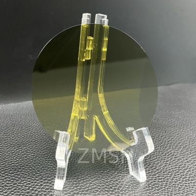
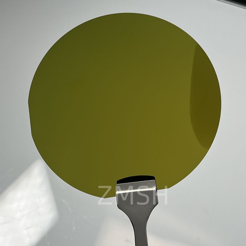
12-inch (300 mm) SiC Epitaxial Wafers are now emerging as the most advanced form factor in the SiC industry. Representing the cutting edge of material science and manufacturing capability, 12” SiC epitaxial wafers offer unparalleled opportunities for scaling up power device production while driving down the cost per device.
As demand for electric vehicles, renewable energy, and industrial power electronics continues to surge globally, 12” wafers are enabling a new generation of SiC MOSFETs, diodes, and integrated power modules with higher throughput, better yield, and lower manufacturing costs.
With wide bandgap properties, high thermal conductivity, and exceptional breakdown voltage, 12” SiC wafers are unlocking new levels of performance and efficiency in advanced power electronics.
![]()
![]()
How 12” SiC Epitaxial Wafers Are Made
Manufacturing 12” SiC epitaxial wafers requires next-generation CVD reactors, precise crystal growth control, and ultra-flat substrate technology:
-
Substrate Fabrication
Monocrystalline 12” SiC substrates are produced via high-temperature sublimation techniques and subsequently polished to sub-nanometer roughness. -
CVD Epitaxial Growth
Advanced large-scale CVD tools operate at ~1600 °C to deposit high-quality SiC epitaxial layers onto the 12” substrates, with optimized gas flow and temperature uniformity to handle the larger area. -
Tailored Doping
N-type or P-type doping profiles are created with high uniformity across the entire 300 mm wafer. -
Precision Metrology
Uniformity control, crystal defect monitoring, and in-situ process management ensure consistency from wafer center to edge. -
Comprehensive Quality Assurance
Each wafer is validated via:-
AFM, Raman, and XRD
-
Full-wafer defect mapping
-
Surface roughness and warp analysis
-
Electrical property measurements
-
Specifications
| Grade | 12InchN-typeSiCSubstrate | ||
| 1 | Polytype | -- | 4HSiC |
| 2 | ConductivityType | -- | N |
| 3 | Diameter | mm | 300.00±0.5mm |
| 4 | Thickness | um | 700±50µm |
| 5 | CrystalSurfaceOrientationAxis | degree | 4.0°toward±0.5° |
| 6 | Notchdepth | mm | 1~1.25mm |
| 7 | Notchorientation | degree | ±5° |
| 8 | Resistivity(Average) | Ωcm | NA |
| 9 | TTV | um | NA |
| 10 | LTV | um | NA |
| 11 | Bow | um | NA |
| 12 | Warp | um | NA |
| 13 | MPD | cm-2 | NA |
| 14 | TSD | cm-2 | NA |
| 15 | BPD | cm-2 | NA |
| 16 | TED | cm-2 | NA |
| 17 | EPD | cm-2 | NA |
| 18 | ForeignPolytypes | -- | NA |
| 19 | SF(BSF)(2x2mmgridsize) | % | NA |
| 20 | TUA(TotalUsableArea)(2x2mmgridsize) | % | NA |
| 21 | NominalEdgeExclusion | mm | NA |
| 22 | Visualscratches | -- | NA |
| 23 | Scratches-cumulativelength(SiSurface) | mm | NA |
| 24 | SiFace | -- | CMPpolished |
| 25 | CFace | -- | CMPpolished |
| 26 | Surfaceroughness(Siface) | nm | NA |
| 27 | Surfaceroughness(Cface) | nm | NA |
| 28 | lasermarking | -- | CFace,abovetheNotch |
| 29 | Edgechip(Front&backSurfaces) | -- | NA |
| 30 | Hexplates | -- | NA |
| 31 | Cracks | -- | NA |
| 32 | Particle(≥0.3um) | -- | NA |
| 33 | Areacontamination(stains) | -- | None:Bothfaces |
| 34 | ResidualMetalsContamination(ICP-MS) | atom/cm2 | NA |
| 35 | EdgeProfile | -- | Chamfer,R-Shape |
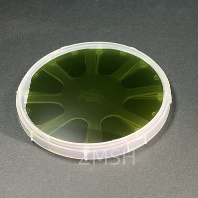
| 36 | Packaging | -- | Multi-waferCassetteOrSingleWaferContainer |
Applications
4” SiC epitaxial wafers enable mass production of reliable power devices in sectors including:
-
Electric Vehicles (EVs)
Traction inverters, onboard chargers, and DC/DC converters. -
Renewable Energy
Solar string inverters, wind power converters. -
Industrial Drives
Efficient motor drives, servo systems. -
5G / RF Infrastructure
Power amplifiers and RF switches. -
Consumer Electronics
Compact, high-efficiency power supplies.
Frequently Asked Questions (FAQ)
1. What is the benefit of 12” SiC wafers?
They significantly reduce production cost per chip through increased wafer area and process yield.
2. How mature is 12” SiC production?
12” is entering pilot production with select industry leaders—our wafers are available now for R&D and volume ramp.
3. Can doping and thickness be customized?
Yes, full customization of doping profile and epi thickness is available.
4. Are existing fabs compatible with 12” SiC wafers?
Minor equipment upgrades are needed for full 12” compatibility.
5. What is typical lead time?
6–10 weeks for initial orders; shorter for repeat volumes.
6. What industries will adopt 12” SiC fastest?
Automotive, renewable energy, and grid infrastructure sectors.
Related Products
![]()
12 inch SiC Wafer 300mm Silicon Carbide wafer Conductive Dummy Grade N-Type Research grade
![]()
4H/6H P-Type Sic Wafer 4inch 6inch Z Grade P Grade D Grade Off Axis 2.0°-4.0° Toward P-type Doping