| Brand Name: | ZMSH |
| Model Number: | Sapphire Wafer |
| MOQ: | 10 PCS |
| Price: | 10usd |
| Packaging Details: | Vacuum Package |
| Payment Terms: | T/T |
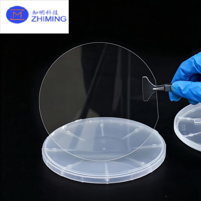
4 Inch Sapphire Wafer, Al2O3 Single Crystal Sapphire Substrate, SSP DSP Polished
Product Description:
4 inch sapphire wafer, single crystal Al₂O₃ substrate. C-plane (0001), SSP / DSP polished, epi-ready grade. Low TTV, ultra-smooth surface, high thermal & chemical stability. Widely used for GaN epitaxy, LED, optoelectronics and optical devices. Custom thickness, orientation and PSS available. Clean packaging, stable supply.
Introduction of Sapphire Wafers:
Sapphire wafer is a single-crystal alumina (Al₂O₃) substrate. It features excellent light transmittance, high thermal conductivity, great chemical resistance and stable mechanical properties.As a mainstream substrate material, it is widely adopted for GaN epitaxy, LED chips, Micro-LED, optical windows and photoelectric sensors. Different crystal orientations including C-plane, R-plane, A-plane and M-plane are available.We supply 4-inch sapphire wafers with SSP or DSP polishing, epi-ready grade. Patterned sapphire substrate (PSS) is also optional. Custom specifications on thickness, tolerance and surface index can be supported. Stable quality and reliable delivery for semiconductor and optoelectronic manufacturers.
Product Parameters:
| Grade | Zero MPD Production Grade (Z Grade) | Dummy Grade (D Grade) |
| Diameter | 99.5 mm - 100.0 mm | 99.5 mm - 100.0 mm |
| Poly-type | 4H | 4H |
| Thickness | 350 μm ± 15 μm | 350 μm ± 25 μm |
| Wafer Orientation | Off axis : 4.0° toward <11-20> ± 0.5° | Off axis : 4.0° toward <11-20> ± 0.5° |
| Micropipe | ≤ 0.2 cm² | ≤ 15 cm² |
| Resistivity | 0.015 - 0.024 Ω·cm | 0.015 - 0.028 Ω·cm |
| Primary Flat Orientation | (10-10) ± 5.0° | (10-10) ± 5.0° |
| Primary Flat Length | 32.5 mm ± 2.0 mm | 32.5 mm ± 2.0 mm |
| Secondary Flat Length | 18.0 mm ± 2.0 mm | 18.0 mm ± 2.0 mm |
| Secondary Flat Orientation | Silicon face up: 90° CW, from Prime flat ± 5.0° | Silicon face up: 90° CW, from Prime flat ± 5.0° |
| Edge Exclusion | 3 mm | 3 mm |
| LTV / TTV / Bow / Warp | ≤ 2.5 μm / ≤ 5 μm / ≤ 15 μm / ≤ 30 μm | ≤ 10 μm / ≤ 15 μm / ≤ 25 μm / ≤ 40 μm |
| Roughness | Polish Ra ≤ 1 nm | Polish Ra ≤ 1 nm |
| CMP Ra ≤ 0.2 nm | CMP Ra ≤ 0.5 nm | |
| Edge Cracks By High Intensity Light | — | Cumulative length ≤ 10 mm single length ≤ 2 mm |
| Hex Plates By High Intensity Light | Cumulative area ≤ 0.05% | Cumulative area ≤ 0.1% |
| Polytype Areas By High Intensity Light | — | Cumulative area ≤ 3% |
| Visual Carbon Inclusions | Cumulative area ≤ 0.05% | Cumulative area ≤ 3% |
| Silicon Surface Scratches By High Intensity Light | — | Cumulative length ≤1 × wafer diameter |
| Edge Chips By High Intensity Light | None permitted ≥ 0.2 mm width and depth | 5 allowed, ≤ 1 mm each |
| Silicon Surface Contamination By High Intensity | — | — |
| Threading Screw Dislocation | ≤ 500 cm² | — |
| Packaging | Multi-wafer Cassette Or Single Wafer Container | Multi-wafer Cassette Or Single Wafer Container |
![]()
![]()
Applications of 4inch Sapphire Wafers:
4-inch single-crystal sapphire wafers balance R&D flexibility and mass-production cost-effectiveness. With outstanding properties including high temperature resistance, excellent insulation, broad-spectrum transmittance and chemical stability, they are widely used in the mass production of optoelectronic devices such as LEDs, Mini/Micro LEDs and laser diodes, as well as semiconductor fields including GaN power devices, 5G RF chips and SOS integrated circuits. They can also be processed into optical windows, sensor substrates, MEMS devices and special industrial components, and serve as a mainstream substrate specification for academic research, pilot process testing and production line transition.
Related Products:
8inch Sapphire Wafer DSP Al2O3 Single Crystal for LED Lighting
![]()
6 Inch Sapphire Based AlN Templates Wafer For 5G BAW Devices Sapphire wafer sapphire window
![]()
Q&A:
Q1: What are sapphire wafers used for?
A1: Sapphire wafers are core substrate materials for third-generation semiconductors and high-end optics. They mainly serve as epitaxial substrates for blue/green LEDs, UV LEDs, Mini/Micro LEDs and laser diodes, and are also widely applied in GaN power devices, 5G RF chips, optical windows and MEMS sensors. They are also commonly used as experimental substrates for university material research and thin film deposition tests.
Q2: How to choose between SSP and DSP sapphire wafers?
A2: SSP (Single-Side Polished) wafers have an epitaxial-grade mirror finish only on the front side with a lapped back side, delivering higher cost-effectiveness. They fit scenarios that only use the front side, such as conventional GaN epitaxy and single-side coating. DSP (Double-Side Polished) wafers feature mirror finishes on both sides with better flatness and parallelism, ideal for double-sided optical transmission, double-sided film deposition and backside optical inspection.
Q3: What is a sapphire wafer?
A3: A sapphire wafer is a single-crystal thin slice made of high-purity single-crystal α-Al₂O₃, processed through crystal orientation, multi-wire slicing, precision lapping and CMP polishing. The mainstream C-plane (0001) orientation comes in SSP and DSP versions. With properties like high temperature resistance, excellent insulation and broad-spectrum transmittance, it is a key foundational material for the semiconductor and optical industries.
ZMSH specializes in high-tech development, production, and sales of special optical glass and new crystal materials. Our products serve optical electronics, consumer electronics, and the. We offer Sapphire optical components, mobile phone lens covers, Ceramics, LT, Silicon Carbide SIC, Quartz, and semiconductor crystal wafers. With skilled expertise and cutting-edge equipment, we excel in non-standard product processing, aiming to be a leading optoelectronic materials high-tech enterprise.
![]()