


|
Large Thickness SiO2 Thermal Oxide On Silicon Wafers For Optical Communication System
Product Details:
| Place of Origin: | CHINA |
| Brand Name: | ZMSH |
| Certification: | ROHS |
| Model Number: | SI WAFER |
Payment & Shipping Terms:
| Minimum Order Quantity: | 10pcs |
|---|---|
| Price: | by quantites |
| Packaging Details: | single wafer container |
| Delivery Time: | 2-4weeks |
| Payment Terms: | Western Union, T/T |
|
Detail Information |
|||
| MATERIAL: | Silicon Wafer And SiO2 | Application: | Star Coupler, Splitter |
|---|---|---|---|
| SiO2 Thick: | 25um +/-6um | Package: | Single Wafer Container |
| High Light: | SiO2 Thermal Oxide Silicon Wafer,Optical Communication System SiO2 Wafer,Semiconductor Silicon On Sapphire Wafers |
||
Product Description
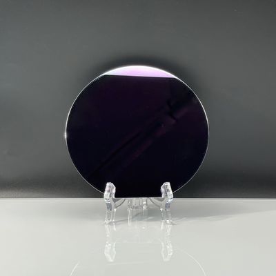
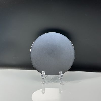
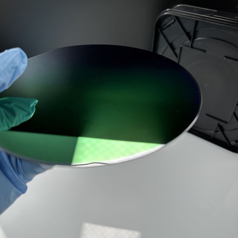
SapphiLarge Thickness Thermal Oxide (SiO2) On Silicon Wafers For Optical Communication System
Generally, the oxide layer thickness of silicon wafers is mainly concentrated below 3um, and the countries and regions that can stably produce high-quality thick oxide layer (above 3um) silicon wafers are still dominated by the United States, Japan, South Korea and Taiwan, China. This project aims to break through the film forming efficiency, film thickness limit and film forming quality of oxide film (SiO) under the current oxide layer growth process, and produce a maximum of 25um(+5%) ultra-thick oxide layer silicon wafer with high quality and high efficiency in a relatively short time. In-plane and inter-plane uniformity +0.5%, refractive index of 1550nm 1.4458+0.0001. Make a contribution to the localization of 5G and optical communication.
The reasons of One day optical communication will replace wired and microwave communication and become the mainstream of communication
- Optical communication devices are the basis of constructing optical communication systems and networks
- Optical passive device is an important part of optical fiber communication equipment, and it is also an indispensable component of other optical fiber applications.
- The optical passive device realizes the functions of connection, energy attenuation, reverse isolation shunt or shunt, signal modulation and filtering in the optical path respectively
- Among them, Splitter (Splitter), Star coupler (Star coupler), Optical switch (Optical switch), wavelength division multiplexer (WDM), array waveguide grating (AWG), etc., are all optical passive devices based on planar optical waveguide technology solutions.
- For optical waveguides, silica (Sio), with good optical, electro-mechanical properties and thermal stability, is considered to be the most practical and promising technical approach for passive optical integration.
The application of Thermal Oxide (SiO2) On Silicon Wafers
- In the context of the rapid development of 5G and optical communication, as well as people's increasing needs for information transmission and exchange, the pursuit of high speed and low delay is endless
- As an excellent carrier of optical path, silicon dioxide (SiO2) has also put forward higher and more demanding requirements for its thickness and purity, and oxide layer silicon is an indispensable material to support optical communication optical devices.
- The countries and regions that can produce thick oxide layer (above 3um) with high quality and stability are still mainly the United States, Japan, South Korea and Taiwan, China.
Production method
Silicon wafers form silica layers through furnace tubes in the presence of oxidizing agents at elevated temperatures, a process known as thermal oxidation. The temperature range is controlled from 900 to 1,250℃; The ratio of the oxidizing gas H2:O2 is between 1.5:1 and 3:1. According to the size of the silicon wafer, there will be different flow loss without oxidation thickness. The substrate silicon wafer is 6 "or 8" monocrystalline silicon with an oxide layer thickness of 0.1μm to 25μm.
Standard Specification
|
Items |
Specification |
| Layer Thickness | 20um士5% |
| Uniformity ( within a wafer) | 土0.5% |
| Uniformity (between wafers) | 土0.5% |
| Refractive Index (@1550nm) | 1.4458+0.0001 |
| Particle | ≤50Measured Average <10 |
![]()
![]()
The details of products
![]()
![]()