


 |
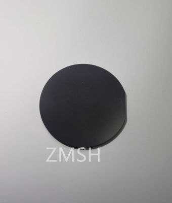
4 Inches 6 Inches 8 Inches SOI Wafers Compatible With CMOS Three Layer Structure
Product Details:
| Place of Origin: | China |
| Brand Name: | ZMSH |
| Model Number: | SOI wafer |
Payment & Shipping Terms:
| Minimum Order Quantity: | 5 |
|---|---|
| Delivery Time: | 2-4 weeks |
| Payment Terms: | T/T |
|
Detail Information |
|||
| Thermal Conductivity: | Relatively High Thermal Conductivity | Performance Advantages: | Superior Electrical Characteristics, Size Reduction, Minimized Crosstalk Between Electronic Devices, Among Others |
|---|---|---|---|
| Active Layer Thickness: | Typically Ranging From A Few To Several Tens Of Nanometers (nm) | Resistivity: | Typically Ranging From Several Hundred To Several Thousand Ohm-centimeters (Ω·cm) |
| Wafer Diameter: | 4 Inches, 6 Inches, 8 Inches, Or Larger | Power Consumption Characteristics: | Low Power Consumption Traits |
| Process Advantages: | Provides Improved Electronic Device Performance And Lower Power Consumption | Impurity Concentration: | Low Impurity Concentration Aimed At Minimizing Electron Mobility Effects |
| High Light: | Silicon On Insulator Wafer Stands,SOI Wafers 4 Inches,CMOS Three Layer Structure SOI Wafers |
||
Product Description
SOI wafers 4 Inches, 6 Inches, 8 Inches, Compatible with CMOS three-layer structure
Product Description:
The SOI (Silicon on Insulator) wafer stands as a pioneering marvel in the realm of semiconductor technology, revolutionizing the landscape of advanced electronics. Comprising three distinct layers, this cutting-edge wafer embodies a trifecta of innovation, offering unparalleled performance, efficiency, and versatility.
At its core lies a three-layer structure. The uppermost layer features a single-crystal silicon layer, known as the Device Layer, serving as the foundation for integrated circuitry. Beneath it resides the Buried Oxide Layer, providing insulation and isolation between the upper silicon layer and the base. Finally, the bottom layer consists of the Handle Layer, forming the substrate upon which this technological masterpiece is built.
One of the standout characteristics of the SOI wafer is its compatibility with CMOS (Complementary Metal-Oxide-Semiconductor) technology. This compatibility seamlessly integrates the benefits of SOI into existing semiconductor manufacturing processes, offering a pathway to enhanced performance without disrupting established production methodologies.
The innovative three-layer composition of the SOI wafer brings forth an array of advantages. It dramatically reduces power consumption, owing to the insulating properties of the Buried Oxide Layer, which minimizes electronic device capacitance and enhances circuit speed and efficiency. This reduction in power consumption not only enhances battery life in portable devices but also contributes to energy-efficient operation in a multitude of applications.
Moreover, the SOI wafer's insulation layer confers superior resistance to radiation, making it exceptionally suited for applications in harsh and high-radiation environments. Its capability to mitigate radiation effects ensures reliability and functionality, even in extreme conditions.
The tri-layer structure also diminishes signal interference, optimizing the performance of integrated circuits by reducing crosstalk between components. This results in improved signal integrity, paving the way for enhanced data processing and communication efficiency.
Additionally, the insulation layer aids in efficient heat dissipation, effectively dispersing heat within the wafer. This feature prevents chip overheating, ensuring sustained performance and longevity of the integrated circuits.
In conclusion, the SOI wafer represents a paradigm shift in semiconductor technology. Its tri-layered architecture, coupled with compatibility with CMOS technology, unlocks a realm of possibilities for high-performance electronics. From power-efficient consumer electronics to robust solutions for aerospace and defense, the SOI wafer's innovative design and multifaceted advantages make it a cornerstone of the ever-evolving world of semiconductor innovation.
Features:
Double-layer structure: The SOI wafer comprises three layers, with the top layer being the single-crystal silicon layer (Device Layer), the middle layer being the insulating layer (Buried Oxide Layer), and the bottom layer being the silicon substrate (Handle Layer).
Low power consumption: Due to the presence of the insulating layer, the SOI wafer exhibits lower power consumption in electronic devices. The insulating layer reduces the capacitance coupling effect between electronic devices, thereby enhancing the speed and efficiency of integrated circuits.
Radiation resistance: The insulating layer of the SOI wafer enhances the silicon's resistance to radiation, enabling better performance in high-radiation environments, making it suitable for specific applications.
Reduced crosstalk: The presence of the insulating layer helps reduce crosstalk between signals, improving the performance of integrated circuits.
Heat dissipation: The insulating layer of the SOI wafer contributes to heat diffusion, enhancing the heat dissipation efficiency of integrated circuits, aiding in preventing chip overheating.
High integration and performance: SOI technology enables chips to have higher integration and performance, allowing electronic devices to accommodate more components within the same size.
CMOS compatibility: SOI wafers are compatible with CMOS technology, benefiting existing semiconductor manufacturing processes.
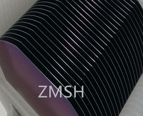
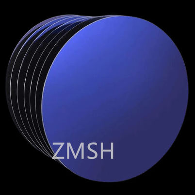
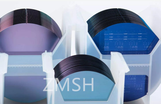
SOI wafers manufacturing
![]()
Technical Parameters:
| Parameters | Values |
|---|---|
| Thickness of Insulating Layer | Approximately Several Hundred Nanometers |
| Resistivity | Typically Ranging From Several Hundred To Several Thousand Ohm-centimeters (Ω·cm) |
| Fabrication Process | Multi-crystalline Silicon Layers Prepared Using A Special Process |
| Active Layer Thickness | Typically Ranging From A Few To Several Tens Of Nanometers (nm) |
| Doping Type | P-type Or N-type |
| Insulating Layer | Silicon Dioxide |
| Crystal Quality between Layers | High-quality Crystal Structure, Contributing To Device Performance |
| SOI Thickness | Usually Within The Range Of Several Hundred Nanometers To A Few Micrometers |
| Process Advantages | Provides Improved Electronic Device Performance And Lower Power Consumption |
| Performance Advantages | Superior Electrical Characteristics, Size Reduction, Minimized Crosstalk Between Electronic Devices, Among Others |
| Conductivity | High |
| Surface oxidation | Available |
| Silicon oxide wafer | Available |
| Epitaxy | Available |
| Doping | P-type Or N-type |
| SOI | Available |
Applications:
Microprocessor and Integrated Circuit Manufacturing: SOI technology plays a pivotal role in the manufacturing of microprocessors and integrated circuits. Its attributes of low power consumption, high performance, and radiation resistance make it an ideal choice for high-performance microprocessors, especially in fields like mobile devices and cloud computing.
Communication and Wireless Technology: The widespread application of SOI technology in the communication sector is due to its ability to reduce power consumption and enhance integration. This includes the manufacturing of high-performance integrated circuits for radio frequency (RF) and microwave devices, as well as efficient chips for 5G and Internet of Things (IoT) devices.
Imaging and Sensor Technology: SOI wafers find significant use in producing image sensors and various sensor types. Their high performance and lower power consumption make them crucial in areas such as cameras, medical imaging equipment, and industrial sensors.
Aerospace and Defense: The radiation-resistant nature of SOI wafers makes them excel in high-radiation environments, leading to crucial applications in aerospace and defense. They are used in manufacturing key components for unmanned aerial vehicles, satellites, navigation systems, and high-performance sensors.
Energy Management and Green Technologies: Due to their low power consumption and high efficiency, SOI wafers also find applications in energy management and green technologies. These include usage in smart grids, renewable energy sources, and energy-saving devices.
Overall, the versatile application of SOI wafers spans across various domains, owing to their unique properties, making them a preferred material for many high-performance electronic devices and systems.
Customization:
Brand Name: ZMSH
Model Number: SOI wafer
Place of Origin: China
The customized Semiconductor Substrate is manufactured with advanced thin film technology, electro-oxidation, conductivity, filtration and doping. It features low contact resistance between layers, high-quality flat surface, reducing defects, low impurity concentration aimed at minimizing electron mobility effects, high-quality crystal structure, contributing to device performance, and strong resistance to radiation.
Support and Services:
We provide comprehensive technical support and service for our Semiconductor Substrate products, including:
- Product selection guidance
- Installation and commissioning
- Maintenance, repairs, and upgrades
- Troubleshooting and problem-solving
- Training and user education
- Product replacement and exchange
Our technical support team is staffed by experienced professionals who are committed to ensuring our customers' satisfaction. We strive to provide quick response times and effective problem resolution.