


 |
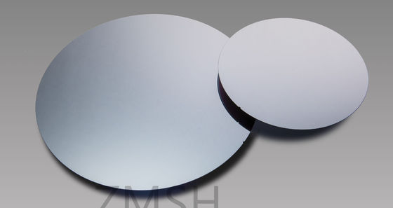
High Purity Silicon Wafers High Thermal Conductivity 3 Inch 4 Inch 6 Inch 8 Inch
Product Details:
| Place of Origin: | China |
| Brand Name: | ZMSH |
| Certification: | ROHS |
| Model Number: | high purity wafer |
Payment & Shipping Terms:
| Minimum Order Quantity: | 10 |
|---|---|
| Delivery Time: | 2-4 weeks |
| Payment Terms: | T/T |
|
Detail Information |
|||
| Material Type: | Single-Crystal Silicon | Purity: | 99.9999% (6N) Or Higher |
|---|---|---|---|
| Crystal Orientation: | <100>, <111>, <110>, Etc. | Flatness: | ≤1μm Or Better |
| Surface Roughness: | <0.5nm RMS Or Lower | Thermal Conductivity: | <10/cm² Or Lower |
| Crystal Defects: | No Slip Bands, No Twins, Etc. | Thickness: | Standard Thickness Or Customized As Per Customer Requirements |
| High Light: | 4 Inch Silicon Wafers,High Purity Silicon Wafers |
||
Product Description
Electronic-Grade Silicon Wafers Ultra-High Purity Optoelectronic-Grade
Abstract
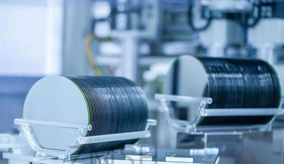
The high-purity silicon wafer we offer undergoes precision machining and strict quality control, meeting the semiconductor industry's high demands for purity and performance. These wafers are made from pure raw materials and optimized growth processes, ensuring extremely low impurity content and excellent crystal quality. Advanced cutting and polishing technologies result in a highly flat wafer surface, providing an ideal substrate for subsequent micro- and nano-processing steps. high-purity silicon wafers possesses high thermal stability and mechanical strength, ensuring stable performance under various process conditions. These features make our high-purity silicon wafer an ideal choice for manufacturing high-performance semiconductor devices.
Application
Quantum Dots: Used for the preparation of quantum dots, applied in displays, photodetectors, etc.
Photolithography Masks: Acts as the base material for masks used in photolithography processes.
Infrared Windows and Lenses: Used to produce infrared windows and lenses, applied in infrared imaging and sensing.
MEMS Devices: high-purity silicon wafers utilized as the base material for various Micro-Electro-Mechanical Systems (MEMS) devices.
Nanoimprint Lithography: Employed in nanoimprint lithography technology to manufacture ultra-precise and ultra-small electronic components.
Quantum Computing: Used in the development and research of quantum computing hardware.
Biocompatible Devices: high-purity silicon wafers utilized to manufacture medical devices and sensors that are compatible with biological tissues.
Feature
Exceptional Purity: Our silicon wafers boast an impressive purity level of 99.9999% (6N) or higher, ensuring optimal performance for your applications.
Precision Manufacturing: With stringent quality control, our wafers have precise thickness, orientation, and surface roughness, meeting the highest industry standards.
High Thermal Conductivity: Our high-purity silicon wafers exhibit excellent thermal conductivity, ensuring efficient heat dissipation for your devices.
Robust Physical Properties: high-purity silicon wafers with superior bending strength and durability, our wafers provide a reliable foundation for your components.
Customizable Options: We offer customizable options for diameter, thickness, and resistivity to meet your specific requirements.
Ultra-Clean Surface: Our wafers undergo meticulous cleaning processes, resulting in an ultra-clean surface with minimal defects.
Consistent Quality: We adhere to rigorous standards to ensure consistent quality across all our products, giving you peace of mind.
Expert Support: Our team of experts is ready to assist you in selecting the perfect wafer specifications for your needs, providing unparalleled support throughout your purchasing journey.
|
Parameter/Feature |
Description/Specification |
|
Material Type |
Single-Crystal Silicon |
|
Purity |
99.9999% (6N) or higher |
|
Diameter |
2 inch, 3 inch, 4 inch, 6 inch, 8 inch, 12 inch, etc. |
|
Thickness |
Standard thickness or customized as per customer requirements |
|
Crystal Orientation |
<100>, <111>, <110>, etc. |
|
Orientation Tolerance |
±0.5° or more precise |
|
Thickness Tolerance |
±5μm or more precise |
|
Flatness |
≤1μm or better |
|
Surface Roughness |
<0.5nm RMS or lower |
|
Bending Strength |
>500MPa |
|
Thermal Conductivity |
<10/cm² or lower |
|
Coefficient of Thermal Expansion |
~2.6 × 10^-6 /°C |
|
Resistivity |
1-100 Ω·cm or customizable |
|
Crystal Defects |
No slip bands, no twins, etc. |
|
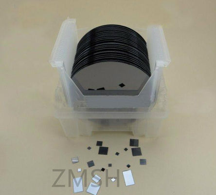
Packaging |
Vacuum packaging in a clean, dust-free environment |
|
Applications |
Semiconductor device manufacturing, optoelectronic devices, high-frequency equipment, micro/nano machining, etc. |
![]()
FAQ:
Q: What's the way of shipping and cost?
A:(1) We accept DHL, Fedex, EMS etc.
(2) it is fine If you have your own express account ,If not,we could help you ship them and
Freight is in accordance with the actual settlement.
Q: How to pay?
A: T/T 100% deposit before delivery.
Q: What's your MOQ?
A: (1) For inventory, the MOQ is 1pcs. if 2-5pcs it's better.
(2) For customized commen products, the MOQ is 10pcs up.
Q: What's the delivery time?
A: (1) For the standard products
For inventory: the delivery is 5 workdays after you place the order.
For customized products: the delivery is 2 -4 weeks after you order contact.
Q: Do you have standard products?
A: Our standard products in stock. as like substrates 4inch 0.35mm.