


|
Beta Coefficient-Ga2O3 Gallium Oxide Wafer Doped Mg Fe3+ Square Substrate Dsp Ssp
Product Details:
| Place of Origin: | China |
| Brand Name: | ZMKJ |
| Model Number: | Beta Coefficient-Ga2O3 |
Payment & Shipping Terms:
| Minimum Order Quantity: | 5pcs |
|---|---|
| Price: | by case |
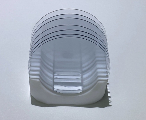
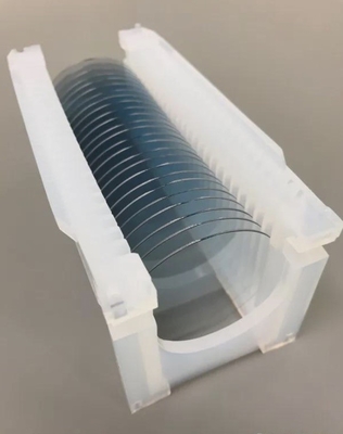
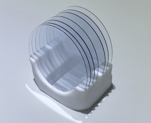
| Packaging Details: | single wafer container in cleaning room |
| Delivery Time: | in 30days |
| Payment Terms: | T/T, Western Union, paypal |
| Supply Ability: | 50pcs/month |
|
Detail Information |
|||
| Layer: | GaN Template | Layer Thickness: | 1-5um |
|---|---|---|---|
| Melt Point (°C): | 1725°C | Conductivity: | Semi-insulating, Fe-doped,Mg-doped |
| Electrical Resistivity: | >1E6 Ohm-cm | Density: | 5.95 G/cm3 |
| High Light: | Beta Coefficient Ga2O3 Gallium Oxide Wafer,Dsp Gallium Oxide Semiconductor Substrate,Square Gallium Oxide Wafer |
||
Product Description
Gallium Oxide Epiwafers Beta Coefficient-Ga2O3 Gallium Oxide Wafer Doped Mg Fe3+ Square Substrate Dsp Ssp
β-Ga2O3 is a gallium oxide compound, which is a wide band gap semiconductor material. Its crystal structure belongs to the hexagonal crystal system, with high electron mobility and large band width, so it has a wide application prospect. Here are some details about β-Ga2O3:
Physical properties:
Crystal structure: hexagonal crystal system
Density: 5.88 g/cm³
Lattice constant: a = 0.121 nm, c = 0.499 nm
Melting point: 1725 °C
Refractive index: 1.9-2.5
Transparent wavelength range: 0.23-6.0μm
Electrical properties:
Band width: 4.8eV
Electron mobility: 200-600 cm²/Vs
Leakage rate: 10^ -5-10 ^-10 A/cm²
REDOX potential: 2.5V vs. NHE
Because of its wide band gap and high electron mobility, β-Ga2O3 has a wide application prospect in power electronics, photoelectronics, solar cells and other fields. Specific applications include:
Ultraviolet detectors and lasers
High power MOSFETs and Schottky diodes
High temperature sensor and potential sensor
Solar cells and LED materials
β-Ga2O3 still faces some challenges in preparation and application, such as crystal growth, impurity control, device fabrication, etc. However, with the continuous development of technology, the application prospect of β-Ga2O3 is still very broad.
| Gallium oxide, Ga2O3 single crystal | 2inch substrates | 10*15mm substrates | |||||
| Orientation | (-201) | (-201) | (-201) | (010) | (010) | (010) | |
| Dopant | Sn | Un-doped | Sn | Sn | Un-doped | Fe | |
| Conductivity | n-type | n-type | n-type | n-type | n-type | Insulation(>1010 | |
| Nd-Na(cm-3) | 5E17~9E18 | 5E17 or less | 5E17~9E18 | 1E18~9E18 | 1E17~5E17 | - | |
| Dimentions | A-B(mm) | 50.8±0.3 | 50.8±0.3 | 15±0.3 | 15±0.3 | 15±0.3 | 15±0.3 |
| C-D(mm) | 41~49.8 | 41~49.8 | 10±0.3 | 10±0.3 | 10±0.3 | 10±0.3 | |
| Thickness | 0.68±0.02 | 0.68±0.02 | 0.68±0.02 | 0.5±0.02 | 0.5±0.02 | 0.5±0.02 | |
| Reference(m | Fig.1 | Fig.1 | Fig.2 | Fig.3 | Fig.3 | Fig.3 | |
| Offset angle (degree) |
[010]:0±0.4 | [010]:0±0.4 | [010]:0±0.4 | 丄[102]:0±1 | 丄[102]:0±1 | 丄[102]:0±1 | |
| [102]:0.7±0.4 | [102]:0.7±0.4 | [102]:0.7±0.4 | [102]:0±1 | [102]:0±1 | [102]:0±1 | ||
| FWHM(arcsec) | [010]:150 or less | [010]:150 or less | [010]:150 or less | 丄[102]:150 or | 丄[102]:150 or | 丄[102]:150 or | |
| [102]:150 or less | [102]:150 or less | [102]:150 or less | [102]:150 or less | [102]:150 or less | [102]:150 or less | ||
| Surface | Front | CMP | CMP | CMP | CMP | CMP | CMP |
| Back | Rough | Rough | Rough | Rough | Rough | Rough |
|
| Item | Specification | |||||
| Orientation | -100 | |||||
| Doped | UID | Mg | Fe | |||
| Electrical parameter | 1 ×10¹⁷~3×1018cm-3 | ≥1010 Ω ·cm | ≥1010 Ω ·cm | |||
| Twin-crystal swing curve half-height width | ≤150 | |||||
| Dislocation density | <1×10 5 cm-2 | |||||
| Dimension | A-B | C-D | 厚度 | |||
| 10mm | 10.5mm | 0.5(±0.02)mm | ||||
| 5mm | 10mm | 0.5(±0.02)mm | ||||
| Flatness | The long side is [010] Orientation | |||||
| Surface | DSP/SSP | |||||
| Ra<0.5nm | ||||||
| Mis<±1. | ||||||
![]()