


 |
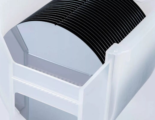
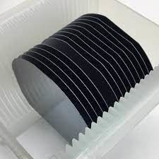
Silicon Wafer CZ orientation111 Resistivity: 1-10 (ohm.cm) single side or double side polish
Product Details:
| Place of Origin: | China |
| Brand Name: | ZMSH |
| Model Number: | si wafer |
Payment & Shipping Terms:
| Payment Terms: | T/T |
|---|
|
Detail Information |
|||
| State Of Matter: | Solid | Melting Point: | 1687K (1414 ℃) |
|---|---|---|---|
| Boiling Point: | 3173K (2900 ° C) | Molar Volume: | 12.06 × 10⁻⁶m3 / Mol |
| Vaporization Heat: | 384.22kJ / Mol | Melting Heat: | 50.55kJ / Mol |
| Vapor Pressure: | 4.77Pa (1683K) | Grade: | Prime |
| Orientation: | <100> <110> <111>±1 | ||
| High Light: | Resistivity: 10 (ohm.cm) Silicon Wafer,Resistivity: 1-10 (ohm.cm) Silicon Wafer,double side polish Silicon Wafer |
||
Product Description
Silicon Wafer CZ orientation111 Resistivity: 1-10 (ohm.cm) single side or double side polish
Product abstract
Our Si wafer offers high purity and exceptional uniformity, ideal for a wide range of semiconductor and photovoltaic applications. With precise control over crystal structure and surface quality, this wafer enables the fabrication of high-performance devices. Whether used in integrated circuits, solar cells, or MEMS devices, our Si wafer delivers reliability and efficiency for demanding applications in various industries.
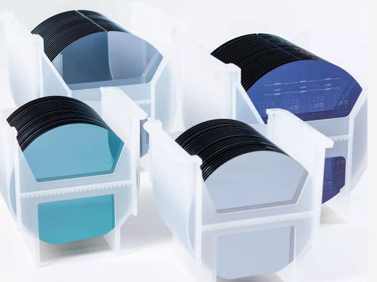
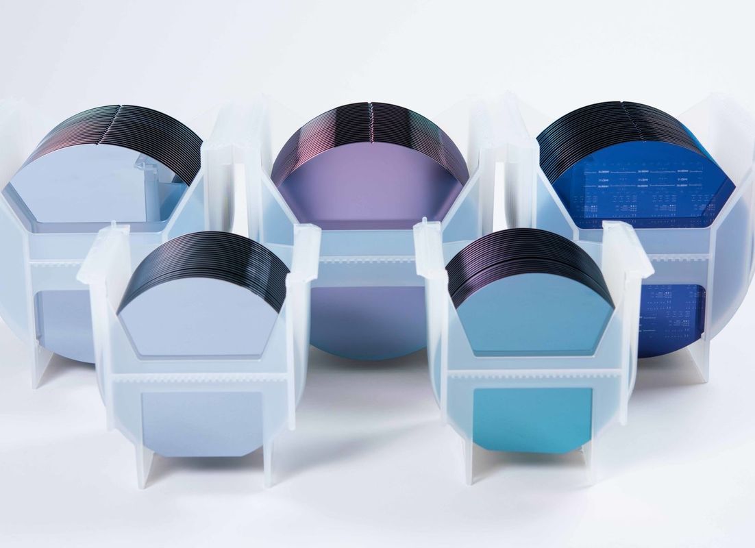
Product showcase
![]()
![]()
Product applications
-
Integrated Circuits (ICs): Our Si wafer serves as the foundational material for the fabrication of integrated circuits used in a wide range of electronic devices, including smartphones, computers, and automotive electronics. It provides a stable platform for the deposition of semiconductor layers and the integration of various electronic components onto a single chip.
-
Photovoltaic (PV) Cells: Our Si wafer is utilized in the production of high-efficiency solar cells for photovoltaic applications. It serves as the substrate for the deposition of semiconductor layers, facilitating the conversion of sunlight into electricity in solar panels and renewable energy systems.
-
MEMS Devices: Our Si wafer enables the fabrication of Microelectromechanical Systems (MEMS) devices such as accelerometers, gyroscopes, and pressure sensors. It provides a stable base for the integration of mechanical and electrical components, allowing for precise sensing and control in various applications.
-
Power Electronics: Our Si wafer is used in power semiconductor devices such as diodes, transistors, and thyristors for power electronics applications. It enables efficient energy conversion and control in electric vehicles, renewable energy systems, and industrial automation equipment.
-
Optoelectronic Devices: Our Si wafer supports the development of optoelectronic devices such as photodetectors, optical modulators, and light-emitting diodes (LEDs). It serves as a platform for the integration of semiconductor materials with optical functionalities, enabling applications in telecommunications, data communication, and optical sensing.
-
Microelectronics: Our Si wafer is essential for the fabrication of various microelectronic devices, including sensors, actuators, and RF components. It provides a stable and uniform substrate for the integration of electronic components with micron-scale dimensions, supporting advancements in consumer electronics, automotive systems, and medical devices.
-
Sensors: Our Si wafer is utilized in the production of sensors for various applications, including environmental monitoring, biomedical sensing, and industrial automation. It enables the fabrication of sensitive and reliable sensor devices for detecting physical, chemical, and biological parameters.
-
Solar Panels: Our Si wafer contributes to the manufacturing of solar panels for renewable energy generation. It serves as the base material for the deposition of semiconductor layers, enabling the conversion of sunlight into electricity through the photovoltaic effect.
-
Semiconductor Devices: Our Si wafer is employed in the production of a wide range of semiconductor devices, including transistors, diodes, and capacitors. It provides a stable and uniform substrate for the integration of semiconductor materials and the fabrication of electronic components for various applications.
-
Microfluidics: Our Si wafer supports the development of microfluidic devices for applications such as lab-on-a-chip systems, biomedical diagnostics, and chemical analysis. It provides a platform for the integration of microchannels, valves, and sensors, enabling precise control and manipulation of fluids at the microscale.
Product properties
-
High Purity: Our Si wafer exhibits high purity, with low levels of impurities and defects, ensuring excellent electrical properties and device performance.
-
Uniform Crystal Structure: The wafer features a uniform crystal structure with minimal defects, enabling consistent device fabrication and reliable operation.
-
Controlled Surface Quality: Each wafer undergoes rigorous surface treatment processes to achieve a smooth and defect-free surface, essential for the deposition of thin films and the formation of device interfaces.
-
Precise Dimensional Control: Our Si wafer is manufactured with precise dimensional control, ensuring uniform thickness and flatness across the entire surface, facilitating accurate device fabrication processes.
-
Customizable Specifications: We offer a range of customizable specifications for our Si wafers, including doping concentration, resistivity, and orientation, to meet the specific requirements of diverse semiconductor applications.
-
High Thermal Stability: The wafer demonstrates high thermal stability, allowing for reliable operation across a wide range of temperatures without compromising device performance.
-
Excellent Electrical Properties: Our Si wafer exhibits excellent electrical properties, including high carrier mobility, low leakage currents, and uniform electrical conductivity, essential for optimizing device performance and efficiency.
-
Compatibility with Semiconductor Processes: The wafer is compatible with various semiconductor processing techniques, including epitaxy, lithography, and etching, enabling seamless integration into existing fabrication workflows.
-
Reliability and Longevity: Designed for long-term reliability, our Si wafer undergoes stringent quality control measures to ensure consistent performance and durability throughout its operational lifespan.
-
Environmentally Friendly: Our Si wafer is environmentally friendly, posing minimal risks to health and the environment during manufacturing and operation, aligning with sustainable manufacturing practices.
-
Specifications of Silicon wafers
Item Unit Specification Grade -- Prime Crystallinity -- Monocrystalline Diameter inches 2 inch or 3 inch or 4 inch or 6 inch or 8 inch Diameter mm 50.8±0.3 or 76.2±0.3 or 100±0.5 or 154±0.5 or 200±0.5 Growth Method CZ / FZ Dopant Boron / Phosphorus Type P / N type Thickness μm 180 – 1000±10 or as required Orientation <100> <110> <111>±1 Resistivity Ω-cm As required Polishing Single side or Double side polished SiO2 layer (grown by thermal oxidation) / Si3N4 layer (grown by LPCVD) layer thickness as required Packing As per requirement