


 |
2inch 3inch 4inch LNOI LiNbO3 Wafer Lithium Niobate Thin Films Layer On Silicon Substrate
Product Details:
| Place of Origin: | China |
| Brand Name: | ZMKJ |
| Certification: | ROHS |
| Model Number: | JZ-2inch 3inch 4inch INCH-LNOI |
Payment & Shipping Terms:
| Minimum Order Quantity: | 1pcs |
|---|---|
| Price: | by case |
| Packaging Details: | single wafer container in cleaning room |
| Delivery Time: | 4 weeks |
| Payment Terms: | T/T, Western Union, paypal |
| Supply Ability: | 10pcs/month |
|
Detail Information |
|||
| Material: | LiNbO3 Layer On Silicon Substrate | Layer Thickness: | 300-1000nm |
|---|---|---|---|
| Orientation: | X-CUT | Ra: | 0.5nm |
| Isolation Layer: | SiO2 | Substrate: | 525um |
| Size: | 2inch 3inch 4inch 8inch | Product Name: | LNOI |
| High Light: | 4inch Lithium Niobate Wafer,Thin Film LNOI Lithium Niobate Wafer,LiNbO3 Silicon Substrate |
||
Product Description
2inch 3inch 4inch LNOI LiNbO3 Wafer Lithium Niobate Thin Films Layer On Silicon Substrate
LNOI wafer preparation process is shown below, including the following five steps:
(1) Ion Implantation: The ion implantation machine is used to drive high-energy He ions from the upper surface of lithium niobate crystal. When He ions with specific energy enter the crystal, they will be obstructed by atoms and electrons in LN crystal and gradually slow down and stay at A specific depth position, destroying the crystal structure near this position and splitting the LN crystal into upper and lower A/B layers. And zone A is going to be the thin film that we need to make LNOI.
(2) Substrate Preparation: To make thin film lithium niobate wafers, it is certainly not possible to leave hundreds of nm LN thin films in a suspended state. Underlying supporting materials are required. In common SOI wafers, the substrate is a layer of silicon wafers with a thickness of more than 500um, and then SiO2 dielectric layer is prepared on the surface. Finally, the monocrystalline silicon thin film is bonded on the upper surface to form SOI wafers. As for LNOI wafers, Si and LN are commonly used substrates, and then SiO2 dielectric layer is prepared by thermal oxygen or PECVD deposition process. If the surface of the dielectric layer is uneven, chemical mechanical grinding CMP process is needed to make the upper surface smooth and smooth, which is convenient for subsequent bonding process.
(3) Film Bonding: Using a wafer bonding device, the ion implanted LN crystal is reversed 180 degrees and bonded to the substrate. For wafer level production, the bonding surfaces of both substrates and LN are smoothed, usually by direct bonding without the need for intermediate binder materials. For scientific research, BCB (benzocyclobutene) can also be used as the intermediate layer binder material to achieve Die to Die bonding. BCB bonding mode has a low requirement on the smoothness of the bonding surface, which is very suitable for scientific research experiments. However, BCBS do not have long-term stability, so BCB bonding is not usually used in wafer production
(4) Annealing and Stripping: After the two crystal surfaces are bonded and extruded, high temperature annealing and stripping process are required. After the surface of the two crystals is fitted, it first maintains A certain time at a specific temperature to strengthen the interface bonding force, and makes the injected ion layer bubble, so that A and B films are gradually separated. Finally, mechanical equipment is used to peel the two films apart, and then gradually reduce the temperature to room temperature to complete the entire annealing and stripping process.
(5) CMP Flattening: After annealing, the surface of the LNOI wafer is rough and uneven. Further CMP flattening is needed to make the film on the wafer surface flat and reduce the surface roughness.
Characteristic Specification
| 300-900 nm Lithium Niobate Thin Films (LNOI) | ||||
| Top Functional Layer | ||||
| Diameter | 3, 4, (6) inch | Orientation | X, Z, Y etc. | |
| Material | LiNbO3 | Thickness | 300-900 nm | |
| Doped (optional) | MgO | |||
| Isolation Layer | ||||
| Material | SiO2 | Thickness | 1000-4000 nm | |
| Substrate | ||||
| Material | Si, LN, Quartz, Fused Silica etc. | |||
| Thickness | 400-500 μm | |||
| Optional Electrode Layer | ||||
| Material | Pt, Au, Cr | Thickness | 100-400 nm | |
| Structure | Above or Under SiO2 Isolation Layer | |||
Application of LN-On-Silicon
1, optical fiber communication, such as waveguide modulator, etc. Compared with traditional products, the volume of devices produced by using this thin film material can be reduced by more than one million times, the integration is greatly improved, the response bandwidth is wide, the power consumption is low, the performance is more stable, and the manufacturing cost is reduced.
2, electronic devices, such as high quality filters, delay lines, etc.
3, information storage, and can realize high density information storage, a 3 inch film information storage capacity of 70 t (100000 CD)
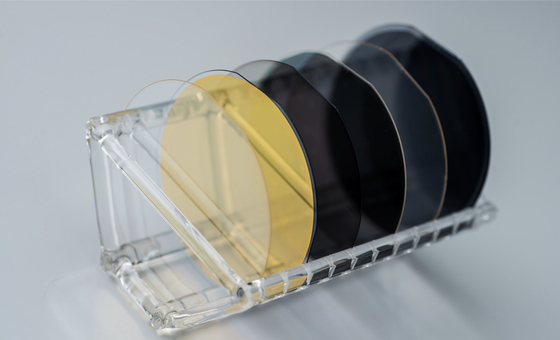
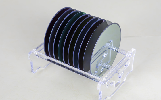
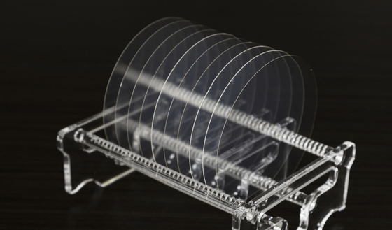
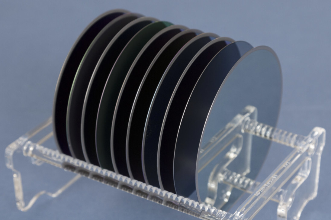
Display of Lithium Niobate Wafer Thin Films Layer On Silicon Substrate
![]()
![]()
![]()