


 |
InAs Wafer Crystal Substrates N Type For MBE 99.9999% Monocrystalline
Product Details:
| Place of Origin: | CHINA |
| Brand Name: | zmkj |
| Certification: | ROHS |
| Model Number: | Indium arsenide (InAs) |
Payment & Shipping Terms:
| Minimum Order Quantity: | 3pcs |
|---|---|
| Price: | by case |
| Packaging Details: | single wafer package in 1000-grade cleaning room |
| Delivery Time: | 2-4weeks |
| Payment Terms: | T/T, Western Union |
| Supply Ability: | 500pcs |
|
Detail Information |
|||
| Material: | Indium Arsenide (InAs) Wafer Substrate | Growth Method: | CZ |
|---|---|---|---|
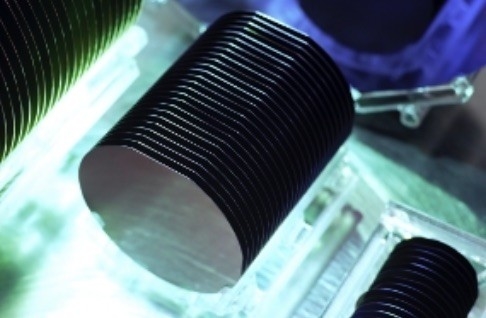
| SIZE: | 2inch 3inch 4inch | Thickness: | 300-800um |
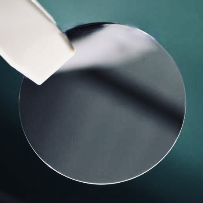
| Application: | III-V Direct Bandgap Semiconductor Material | Surface: | Polished Or Etched |
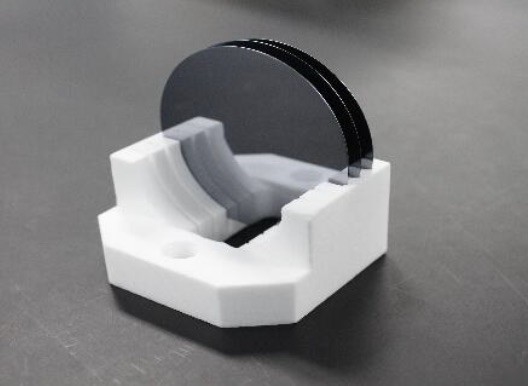
| Package: | Single Wafer Box | Type: | N-type And P-type |
| High Light: | InAs Wafer Crystal Substrates,N Type InAs Wafer,MBE InAs substrate |
||
Product Description
2inch 3inch 4inch InAs Wafer Crystal Substrates N-Type For MBE 99.9999% Monocrystalline
Introduce of InAs substrate
Indium InAs or indium mono-arsenide is a semiconductor composed of indium and arsenic. It has the appearance of a gray cubic crystal with a melting point of 942°C. Indium arsenide is used to construct infrared detectors with a wavelength range of 1-3.8um. The detector is usually a photovoltaic photodiode. Cryogenic cooling detectors have lower noise, but InAs detectors can also be used for high-power applications at room temperature. Indium arsenide is also used to make diode lasers. Indium arsenide is similar to gallium arsenide and is a direct band gap material. Indium arsenide is sometimes used with indium phosphide. Alloy with gallium arsenide to form indium arsenic - a material whose band gap depends on the In/Ga ratio. This method is mainly similar to alloying indium nitride with gallium nitride to produce indium nitride. Indium arsenide is known for its high electron mobility and narrow band gap. It is widely used as a terahertz radiation source because it is a powerful light-amber emitter.
Features of InAs wafer:
♦ With high electron mobility and mobility ratio (μe/μh=70), it is an ideal material for Hall devices.
♦ MBE can be grown with GaAsSb, InAsPSb, and InAsSb multi-epitaxial materials.
♦ Liquid sealing method (CZ), ensure the purity of the material can reach 99.9999% (6N).
♦ All substrates are precisely polished and filled with a protective atmosphere to meet the requirements of Epi-Ready.
♦Crystal direction selection: Another crystal direction is available, e.g. (110).
♦ Optical measurement techniques, such as ellipsometry, ensure a clean surface on each substrate.
![]()
| InAs Wafer Specifications | ||||||||||
| Diameter Slices | 2" | 3" | ||||||||
| Orientation | (100) +/-0.1° | (100) +/- 0.1° | ||||||||
| Diameter (mm) | 50.5 +/- 0.5 | 76.2 +/- 0.4 | ||||||||
| Flat Option | EJ | EJ | ||||||||
| Flat Tolerance | +/- 0.1° | +/- 0.1° | ||||||||
| Major Flat Length (mm) | 16 +/- 2 | 22 +/- 2 | ||||||||
| Minor Flat Length (mm) | 8 +/- 1 | 11 +/- 1 | ||||||||
| Thickness (um) | 500 +/- 25 | 625 +/- 25 | ||||||||
| Electrical and Dopant Specifications | ||||||||||
| Dopant | Type | Carrier Concentration cm-3 | Mobility cm^2•V^-1•s^-1 | |||||||
| Undoped | n-type | (1-3)*10^16 | >23000 | |||||||
| Low Sulphur | n-type | (4-8)*10^16 | 25000-15000 | |||||||
| High Sulphur | n-type | (1-3)*10^18 | 12000-7000 | |||||||
| Low Zinc | p-type | (1-3)*10^17 | 350-200 | |||||||
| High Zinc | p-type | (1-3)*10^18 | 250-100 | |||||||
| E.P.D. cm^-2 | 2" <= 15,000 3" <= 50,000 | |||||||||
| Flatness Specifications | ||||||||||
| Wafer Form | 2" | 3" | ||||||||
| Polish/Etched | TTV(um) | <12 | <15 | |||||||
| Bow(um) | <12 | <15 | ||||||||
| Warp(um) | <12 | <15 | ||||||||
| Polish/Polish | TTV(um) | <12 | <15 | |||||||
| Bow(um) | <12 | <15 | ||||||||
| Warp(um) | <12 | <15 | ||||||||
![]()
![]()
![]()
![]()
---FAQ –
Q: Are you a trading company or manufacturer?
A: zmkj is a trading company but has a sapphire manufacturer
as a supplier of semiconductor materials wafers for a wide span of applications.
Q: How long is your delivery time?
A: Generally it is 5-10 days if the goods are in stock. or it is 15-20 days if the goods are not
in stock, it is according to quantity.