


 |
300 - 900nm LN-On-Silicon LiNbO3 Lithium Niobate Wafer Thin Films Layer On Silicon Substrate
Product Details:
| Place of Origin: | China |
| Brand Name: | ZMKJ |
| Certification: | ROHS |
| Model Number: | JZ-4INCH-LNOI |
Payment & Shipping Terms:
| Minimum Order Quantity: | 2pcs |
|---|---|
| Price: | by case |
| Packaging Details: | single wafer container in cleaning room |
| Delivery Time: | 4 weeks |
| Payment Terms: | T/T, Western Union, paypal |
| Supply Ability: | 10pcs/month |
|
Detail Information |
|||
| Material: | LiNbO3 Layer On Silicon Substrate | Layer Thickness: | 300-1000nm |
|---|---|---|---|
| Orientation: | X-CUT | Application 2: | 5G Saw/BAW Devices |
| Ra: | 0.5nm | Isolation Layer: | SiO2 |
| Substrate: | 525um | Size: | 4inch 6inch 8inch |
| High Light: | 900nm LN-On-Silicon Substrate,Thin Films Lithium Niobate Wafer,6inch Lithium Niobate Wafer |
||
Product Description
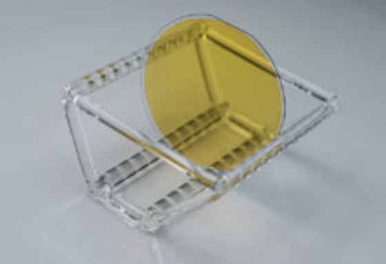
300-900nm LN-On-Silicon LiNbO3 Lithium Niobate Wafer Thin Films Layer On Silicon Substrate
Lithium niobate (LiNbO3) crystal is an important photoelectric material, and is widely used in integrated optics, nonlinear optics, optoelectronic components, and other fields, one of the most important substrate materials. At present, lithium niobate crystals are widely used in surface acoustic wave, electro-optical modulation, laser Q-switching, optical gyro, optical parametric oscillation, optical parametric amplification, optical holographic storage, and other devices, which play an important role in mobile phones, television, optical communication, laser ranging, electric field detector and other devices.
Our production of lithium niobate single crystal thin film has a single crystal lattice structure, maintaining the physical properties of the bulk material, with a diameter of 3 inches, the thickness of the upper lithium niobate single crystal thin film is 0.3-0.7 microns, the middle layer is 1-micron thick silica (SiO2), and the bottom layer is 0.5 mm thick lithium niobate wafer substrate.
Characteristic Specification
| 300-900 nm Lithium Niobate Thin Films (LNOI) | ||||
| Top Functional Layer | ||||
| Diameter | 3, 4, (6) inch | Orientation | X, Z, Y etc. | |
| Material | LiNbO3 | Thickness | 300-900 nm | |
| Doped (optional) | MgO | |||
| Isolation Layer | ||||
| Material | SiO2 | Thickness | 1000-4000 nm | |
| Substrate | ||||
| Material | Si, LN, Quartz, Fused Silica etc. | |||
| Thickness | 400-500 μm | |||
| Optional Electrode Layer | ||||
| Material | Pt, Au, Cr | Thickness | 100-400 nm | |
| Structure | Above or Under SiO2 Isolation Layer | |||
Related Customized Thin Films
| Customized Lithium Niobate & Lithium Tantalate Thin Films | ||||||||
| Top Layer/ Details | Substrate Details | Top Layer Thin Films Details | ||||||
| Multi Layer Structure | Patterned Electrode & Waveguide | Different Material (SiO2/Si, Si, Sapphire, Quartz etc.) | PPLN | Special Size | Electrode (Au, Pt, Cr, Al etc.) | Orientation (Same as Bulk Wafers ) | Doped (MgO, Fe, Er, Tm etc.) | |
| 100-1000 nm LiNbO3 | √ | √ | √ | √ | √ | √ | √ | √ |
| 100-1500 nm LiTaO3 | √ | √ | √ | √ | √ | √ | √ | |
|
5-50 um LiNbO3 |
√ | √ | √ | √ | ||||
|
5-50 um LiTaO3 |
√ | √ | √ | √ | ||||
Application of LN-On-Silicon
1, optical fiber communication, such as waveguide modulator, etc. Compared with traditional products, the volume of devices produced by using this thin film material can be reduced by more than one million times, the integration is greatly improved, the response bandwidth is wide, the power consumption is low, the performance is more stable, and the manufacturing cost is reduced.
2, electronic devices, such as high quality filters, delay lines, etc.
3, information storage, and can realize high density information storage, a 3 inch film information storage capacity of 70 t (100000 CD)
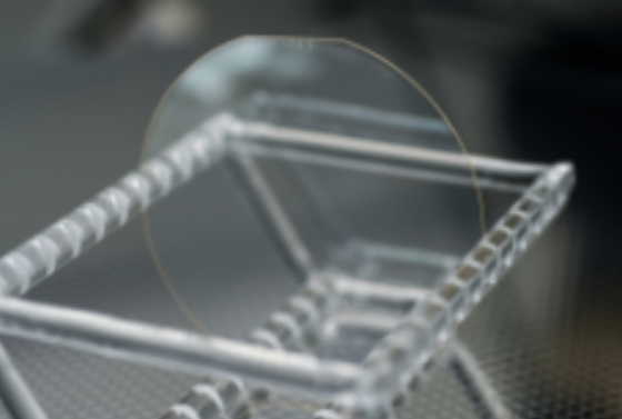
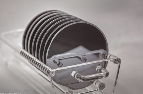
Display of Lithium Niobate Wafer Thin Films Layer On Silicon Substrate
![]()
![]()