

 english
 français
 Deutsch
 Italiano
 Русский
 Español
 português
 Nederlandse
 ελληνικά
 日本語
日本語
 한국
한국
 العربية
 हिन्दी
 Türkçe
 indonesia
 tiếng Việt
 ไทย
ไทย
 বাংলা
বাংলা
 فارسی
فارسی
 polski
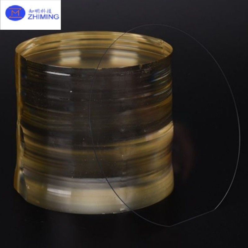
LNOI (Lithium Niobate on Insulator) wafers are utilized in a wide range of advanced applications due to their exceptional properties, including high nonlinear optical coefficients and strong mechanical characteristics. In integrated optics, LNOI wafers are essential for creating photonic devices such as modulators, waveguides, and resonators, which are critical for manipulating light in integrated circuits. In telecommunications, LNOI wafers are widely used in optical modulators, which enable high-speed data transmission in fiber-optic networks. In the field of quantum computing, LNOI wafers play a vital role in generating entangled photon pairs, which are fundamental for quantum key distribution (QKD) and secure communication. Additionally, LNOI wafers are utilized in various sensor applications, where they are used to create highly sensitive optical and acoustic sensors for environmental monitoring, medical diagnostics, and industrial processes. These diverse applications make LNOI wafers a key material in the development of next-generation technologies across multiple fields.
FAQ of LNOI Wafer
Q:What is LNOI?
A:LNOI stands for Lithium Niobate on Insulator. It refers to a type of wafer that features a thin layer of lithium niobate (LiNbO₃) bonded to an insulating substrate like silicon or another insulating material. LNOI wafers retain the excellent optical, piezoelectric, and pyroelectric properties of lithium niobate, making them ideal for use in various photonic, telecommunications, and quantum technologies.
Q:What are the main applications of LNOI wafers?
A:LNOI wafers are used in a variety of applications, including integrated optics for photonic devices, optical modulators in telecommunications, entangled photon generation in quantum computing, and in sensors for optical and acoustic measurements in environmental monitoring, medical diagnostics, and industrial testing.
Q:How are LNOI wafers fabricated?
A:The fabrication of LNOI wafers involves several steps, including ion implantation, bonding of the lithium niobate layer to a substrate (usually silicon), annealing for separation, and chemical mechanical polishing (CMP) to achieve a smooth, high-quality surface. The ion implantation creates a thin, fragile layer that can be separated from the bulk lithium niobate crystal, leaving behind a thin, high-quality lithium niobate film on the substrate.
Related products
![]()
Lithium Niobate (LiNbO3) Crystal EO/PO Components Telecom Defense High-Frequency SAW
![]()
SiC-on-Insulator SiCOI Substrates High Thermal Conductivity Wide Bandgap