


 |
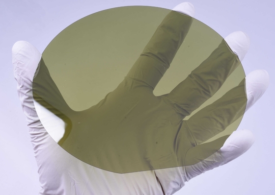
6inch 150mm SIC Wafer 4H-N Type SiC Substrate Dummy Production And Zero Grade
Product Details:
| Place of Origin: | CHINA |
| Brand Name: | ZMKJ |
| Certification: | ROHS |
| Model Number: | 6inch 150mm SiC Substrate |
Payment & Shipping Terms:
| Minimum Order Quantity: | 2pcs |
|---|---|
| Price: | by case |
| Packaging Details: | single wafer package in 100-grade cleaning room |
| Delivery Time: | 1-6weeks |
| Payment Terms: | T/T, Western Union, MoneyGram |
| Supply Ability: | 1-500pcs/month |
|
Detail Information |
|||
| Material: | SiC Single Crystal 4H-N 4H-Si | Grade: | Production Dummy And Zero MPD |
|---|---|---|---|
| Thicnkss: | 0.35mm And 0.5mm | LTV/TTV/Bow Warp: | ≤5 Um/≤15 U/$40 Um/≤60 Um |
| Application: | For MOS And Semiconductor | Diameter: | 6inch 150mm |
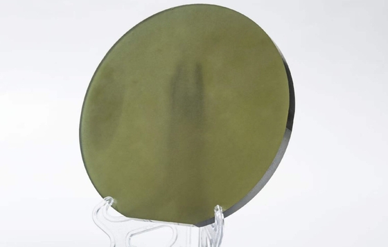
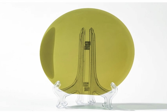
| Color: | Green Tea | MPD: | <2cm-2 For Zero MPD Production Grade |
| High Light: | 150mm SIC Wafer,4H-N Type SiC Substrate,Zero Grade Silicon Carbide Wafer |
||
Product Description
Silicon Carbide (SiC) Substrates 4H and 6H Epi-Ready SiC Substrate/Wafers (150mm, 200mm) Silicon Carbide(SiC) wafer N Type
6inch SIC Wafer 4H-N Type production grade sic epitaxial wafers GaN layer on sic
About Silicon Carbide (SiC)Crystal
Shanghai Famous Trade Co., Ltd 150 mm SiC wafers offer device manufacturers a consistent, high-quality substrate for developing high-performance power devices. Our SiC substrates are produced from crystal ingots of the highest quality using proprietary state-of-the-art physical vapor transport (PVT) growth techniques and computer-aided manufacturing (CAM). Advanced wafer manufacturing techniques are used to convert ingots into wafers to ensure the consistent, reliable quality you need.
Key features
- Optimizes targeted performance and total cost of ownership for next-generation power electronics devices
- Large diameter wafers for improved economies of scale in semiconductor manufacturing
- Range of tolerance levels to meet specific device fabrication needs
- High crystal quality
- Low defect densities
Sized for improved production
With the 6inch 150 mm SiC wafer size, we offer manufacturers the ability to leverage improved economies of scale compared with 100 mm device fabrication. Our 6inch 150 mm SiC Wafers offer consistently excellent mechanical characteristics to ensure compatibility with existing and developing device fabrication processes.
| 6inch 200mm N-Type SiC Substrates Specifications | ||||
| Property | P-MOS Grade | P-SBD Grade | D Grade | |
| Crystal Specifications | ||||
| Crystal Form | 4H | |||
| Polytype Area | None Permitted | Area≤5% | ||
| (MPD) a | ≤0.2 /cm2 | ≤0.5 /cm2 | ≤5 /cm2 | |
| Hex Plates | None Permitted | Area≤5% | ||
| Hexagonal Polycrystal | None Permitted | |||
| Inclusions a | Area≤0.05% | Area≤0.05% | N/A | |
| Resistivity | 0.015Ω•cm—0.025Ω•cm | 0.015Ω•cm—0.025Ω•cm | 0.014Ω•cm—0.028Ω•cm | |
| (EPD)a | ≤4000/cm2 | ≤8000/cm2 | N/A | |
| (TED)a | ≤3000/cm2 | ≤6000/cm2 | N/A | |
| (BPD)a | ≤1000/cm2 | ≤2000/cm2 | N/A | |
| (TSD)a | ≤600/cm2 | ≤1000/cm2 | N/A | |
| (Stacking Fault) | ≤0.5% Area | ≤1% Area | N/A | |
| Surface Metal Contamination | (Al, Cr, Fe, Ni, Cu, Zn, Pb, Na, K, Ti, Ca ,V, Mn) ≤1E11 cm-2 | |||
| Mechanical Specifications | ||||
| Diameter | 150.0 mm +0mm/-0.2mm | |||
| Surface Orientation | Off-Axis:4°toward <11-20>±0.5° | |||
| Primary Flat Length | 47.5 mm ± 1.5 mm | |||
| Secondary Flat Length | No Secondary Flat | |||
| Primary Flat Orientation | <11-20>±1° | |||
| Secondary Flat Orientation | N/A | |||
| Orthogonal Misorientation | ±5.0° | |||
| Surface Finish | C-Face:Optical Polish,Si-Face:CMP | |||
| Wafer Edge | Beveling | |||
| Surface Roughness (10μm×10μm) | Si Face Ra≤0.20 nm ; C Face Ra≤0.50 nm | |||
| Thickness a | 350.0μm± 25.0 μm | |||
| LTV(10mm×10mm)a | ≤2μm | ≤3μm | ||
| (TTV)a | ≤6μm | ≤10μm | ||
| (BOW) a | ≤15μm | ≤25μm | ≤40μm | |
| (Warp) a | ≤25μm | ≤40μm | ≤60μm | |
| Surface Specifications | ||||
| Chips/Indents | None Permitted ≥0.5mm Width and Depth | Qty.2 ≤1.0 mm Width and Depth | ||
| Scratches a (Si Face,CS8520) | ≤5 and Cumulative Length≤0.5×Wafer Diameter | ≤5 and Cumulative Length≤1.5× Wafer Diameter | ||
| TUA(2mm*2mm) | ≥98% | ≥95% | N/A | |
| Cracks | None Permitted | |||
| Contamination | None Permitted | |||
| Edge Exclusion | 3mm | |||
![]()
![]()
![]()
CATALOGUE COMMON SIZE In OUR INVENTORY LIST
4H-N Type / High Purity SiC wafer/ingots 2 inch 4H N-Type SiC wafer/ingots 3 inch 4H N-Type SiC wafer 4 inch 4H N-Type SiC wafer/ingots 6 inch 4H N-Type SiC wafer/ingots | 2 inch 4H Semi-insulating SiC wafer 3 inch 4H Semi-insulating SiC wafer 4 inch 4H Semi-insulating SiC wafer 6 inch 4H Semi-insulating SiC wafer |
6H N-Type SiC wafer 2 inch 6H N-Type SiC wafer/ingot | Customzied size for 2-6inch |
>Packaging – Logistics
Concerns about each detail of the package, cleaning, anti-static, and shock treatment.
According to the quantity and shape of the product, we will take a different packaging process! Almost by single wafer cassettes or 25pcs cassettes in the 100-grade cleaning room.