logo
Good price  online

products details

Created with Pixso. Home Created with Pixso. Products Created with Pixso.
Sapphire Substrate
Created with Pixso.

Sapphire Carriers for Precision Wafer Support and Advanced Semiconductor Manufacturing

Sapphire Carriers for Precision Wafer Support and Advanced Semiconductor Manufacturing

Brand Name: ZMSH
MOQ: 2
Price: 20USD
Packaging Details: custom cartons
Payment Terms: T/T
Detail Information
Place of Origin:
China
Supply Ability:
By case
Product Description

Product Description

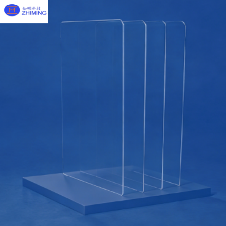
Our Custom Sapphire Carriers are precision-engineered substrates designed to provide reliable mechanical support for wafers, semiconductor dies, and panels during advanced manufacturing and packaging processes. Fabricated from single-crystal sapphire (Al₂O₃), these carriers combine high stiffness, exceptional hardness, optical transparency, and excellent dimensional stability to meet the demanding requirements of precision semiconductor applications.


As wafer-level processing and advanced packaging technologies continue to evolve, carrier substrates must maintain their structural integrity while supporting increasingly thin wafers and complex device structures. Sapphire is a suitable material for applications requiring high rigidity, controlled thickness variation, excellent surface quality, and resistance to mechanical wear.


With a Young’s modulus of approximately 345–420 GPa, sapphire provides a rigid support platform that helps minimize deformation under appropriate processing conditions. Its optical transmittance of over 83% within the specified 300–1200 nm wavelength range also makes it suitable for selected applications requiring optical inspection, alignment, or laser-assisted processing.


Sapphire Carriers for Precision Wafer Support and Advanced Semiconductor Manufacturing


Key Product Advantages

1. High Mechanical Stiffness

Sapphire offers excellent rigidity compared with many conventional carrier materials. This characteristic helps maintain dimensional stability during wafer handling, back grinding, molding, and redistribution layer (RDL) fabrication. It is particularly valuable when processing thin substrates that require stable mechanical support.

Sapphire Carriers for Precision Wafer Support and Advanced Semiconductor Manufacturing2. Excellent Hardness and Surface Durability

With a Mohs hardness of approximately 9, sapphire provides strong resistance to scratching and surface wear. Its durable surface supports precision handling and helps preserve surface quality during processing. Careful handling remains essential to prevent edge chipping and impact damage.

3. High Optical Transparency

The optical transparency of sapphire supports applications involving optical alignment, visual inspection, and selected laser-assisted processing methods. Actual compatibility with laser debonding depends on the wavelength, bonding layer, and release process.

4. Precision Thickness and Flatness Control

Carrier thickness uniformity, surface finish, and warpage can directly influence bonding quality and process consistency. Our custom sapphire carriers can be manufactured to specified dimensional and surface requirements, helping customers achieve reliable support and repeatable processing conditions.

5. Thermal and Chemical Stability

Sapphire offers good thermal stability and resistance to many chemical environments. These properties make it suitable for selected semiconductor processing conditions involving elevated temperatures or chemical exposure. Final material selection should consider the complete process environment and any temporary bonding materials.

Semiconductor Applications

Custom sapphire carriers can be designed for a range of semiconductor processing and advanced packaging applications:

  • Wafer-Level Packaging: Supporting wafer handling, thinning, and subsequent fabrication steps.

  • Fan-Out Packaging: Providing a stable platform for selected die assembly, molding, and interconnection processes.

  • Redistribution Layer Processing: Supporting RDL fabrication where carrier stability and surface quality are important.

  • Mold-First Packaging: Accommodating suitable face-up and face-down processing configurations.

  • Ultra-Thin Wafer Handling: Providing mechanical support during back grinding and precision transfer.

  • Panel-Level Packaging: Supporting selected rectangular or square panel formats.

  • Optical and Laser-Assisted Processes: Providing optical access for compatible inspection, alignment, and release systems.

Application suitability depends on the process flow, bonding configuration, equipment, and required carrier specifications.

Customized Dimensions and Specifications

We offer customized sapphire carrier solutions based on customer drawings, wafer dimensions, and process requirements. Available options may include:

Parameter Description
Material Single-crystal sapphire (Al₂O₃)
Carrier Format Circular wafer, square panel, or rectangular panel
Thickness Reference range: 0.7–2.0 mm
Mechanical Properties High stiffness and hardness
Optical Properties High transmittance within the specified wavelength range
Surface Finish Customized polishing and roughness requirements
Thickness Uniformity Customized TTV requirements
Warpage Specified according to carrier size and application
Edge Configuration Customized edge finishing and geometry
Manufacturing Drawing-based customization available


A Reliable Material for Precision Processing

The combination of high stiffness, surface hardness, optical transparency, and dimensional stability makes sapphire an attractive option for specialized carrier applications. By tailoring the carrier geometry, thickness, surface finish, and tolerance requirements, manufacturers can select a support substrate suited to their specific semiconductor processing needs.


Our custom sapphire carriers are developed for applications where material quality and precision engineering are essential. Whether used for wafer support, advanced packaging development, or specialized optical processing, each design can be evaluated according to its intended operating conditions.


Sapphire Carriers for Precision Wafer Support and Advanced Semiconductor Manufacturing

Sapphire Carrier FAQ

1. What is a sapphire carrier used for in semiconductor manufacturing?

A sapphire carrier is a precision support component used to hold and stabilize wafers, dies, or panels during semiconductor processing. It is suitable for applications such as wafer thinning, temporary bonding, molding, redistribution layer (RDL) fabrication, and advanced packaging, where mechanical stability and dimensional accuracy are important.

2. Why is sapphire selected as a carrier material?

Sapphire is a single-crystal form of aluminum oxide (Al₂O₃). It combines high mechanical stiffness, excellent hardness, optical transparency, and good thermal and chemical stability. These properties make sapphire a suitable material for demanding processing environments where conventional carrier materials may not meet specific mechanical or surface requirements.

3. What are the key material properties of sapphire carriers?

The key properties include:

  • High Young’s modulus: Approximately 345–420 GPa, providing excellent rigidity.

  • High hardness: Mohs hardness of approximately 9, offering strong scratch resistance.

  • Optical transparency: Transmittance exceeding 83% across the specified 300–1200 nm wavelength range.

  • Thermal stability: Suitable for various elevated-temperature processing environments, subject to process conditions.

  • Chemical resistance: Resistant to many chemicals commonly encountered in industrial processing.