logo
Good price  online

products details

Created with Pixso. Home Created with Pixso. Products Created with Pixso.
Sapphire Substrate
Created with Pixso.

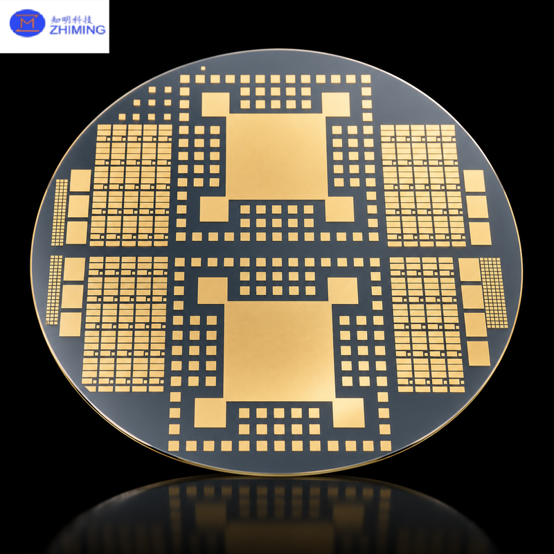
Metallized Sapphire Substrates RF and Microwave Microelectronic Devices

Metallized Sapphire Substrates RF and Microwave Microelectronic Devices

Brand Name: ZMSH
MOQ: 2
Price: 20USD
Packaging Details: custom cartons
Payment Terms: T/T
Detail Information
Place of Origin:
China
Substrate Material:
Single-Crystal Sapphire (Al₂O₃)
Crystal Orientation:
C-Plane (0001), A-Plane (11-20), R-Plane (1-102), Or Custom
Substrate Shape:
Round, Square, Rectangle, Or Custom
Metallization Process:
Sputtering, Evaporation, Or Other Qualified Processes
Adhesion Layer:
Ti, Cr, Or Other Specified Materials
Barrier Layer:
Ni, Pt, Or Other Materials, Depending On Design
Supply Ability:
By case
Highlight:

Metallized sapphire substrates for RF devices

,

Microwave microelectronic sapphire substrates

,

Sapphire substrates with metallized coating

Product Description

Product Overview

Metallized sapphire substrates are functional substrate materials manufactured by depositing metallic thin films onto high-purity single-crystal sapphire (Al₂O₃). By combining the excellent electrical insulation, high hardness, chemical stability, and thermal stability of sapphire with the functional properties of metal films, these substrates provide a versatile solution for advanced electronic devices, RF components, optoelectronic systems, and semiconductor packaging applications.


Depending on specific application requirements, various metals, including titanium (Ti), chromium (Cr), nickel (Ni), gold (Au), and platinum (Pt), can be incorporated into single-layer or multilayer metallization structures. The metal stack can be customized to meet requirements for film adhesion, electrical conductivity, solderability, bonding, and electrical interconnection.


Metallized Sapphire Substrates RF and Microwave Microelectronic Devices      Metallized Sapphire Substrates RF and Microwave Microelectronic Devices

Key Features and Advantages

1. Excellent Electrical Insulation

Sapphire offers excellent electrical insulation, making it suitable for electronic applications that require electrical isolation, stable substrate properties, and reliable structural support.

Metallized Sapphire Substrates RF and Microwave Microelectronic Devices2. High Thermal Stability

Sapphire provides good thermal stability and relatively high thermal conductivity compared with many conventional insulating materials. It is suitable for applications requiring stable substrate performance under demanding thermal conditions. Actual heat dissipation depends on substrate dimensions, metallization design, interface quality, and overall device architecture.

3. Reliable Metal-to-Substrate Interface

With an appropriate adhesion layer and carefully designed metallization stack, the bonding performance between the metal films and sapphire substrate can be optimized. Additional functional or barrier layers can be incorporated to meet specific requirements for soldering, bonding, and electrical connectivity.

4. Flexible Metallization Design

Single-layer and multilayer metal structures are available to accommodate different application requirements. Customization options may include metal composition, film thickness, metallized area, and patterned metallization geometry.

5. Precision Fabrication and Customization

Metallized sapphire substrates can be manufactured according to customer specifications, including substrate dimensions, thickness, surface finish, and metallization patterns. Available tolerances and achievable specifications depend on the selected fabrication process and product design.

Applications

RF and Microwave Devices

Suitable for selected RF and microwave components that require an insulating substrate combined with conductive metal patterns or interconnection structures.

Optoelectronic Devices

Can be used in selected optoelectronic assemblies, electrode structures, mounting substrates, and functional optical components.

Semiconductor Packaging

Applicable to customized metallized carriers, interconnection structures, and packaging components that require the combination of sapphire and metal thin films.

Sensors and Microelectronic Devices

Suitable for sensor platforms and miniature electronic structures requiring an insulating base with functional metal layers.

Customized Electronic Components

Designed for specialized applications that integrate sapphire substrates with tailored metallization structures to meet specific electrical, mechanical, or packaging requirements.

Customization Options

We offer customized metallized sapphire substrate solutions based on customer drawings, device architecture, and application requirements.

  • Substrate specifications: Custom dimensions, thicknesses, and crystal orientations

  • Metallization materials: Selection of suitable metals and multilayer combinations

  • Metal film thickness: Customized layer thicknesses according to design requirements

  • Metallization patterns: Full-surface coating, selective metallization, and patterned metal areas, subject to process feasibility

  • Surface and dimensional specifications: Customized surface finish, dimensional tolerances, and inspection requirements

  • Prototyping and production: Technical evaluation for prototype development and volume manufacturing

Detailed specifications and manufacturing feasibility can be confirmed based on the required design and production process.


Technical Specifications of Metallized Sapphire Substrates

Parameter Specification
Substrate Material Single-Crystal Sapphire (Al₂O₃)
Crystal Orientation C-Plane (0001), A-Plane (11-20), R-Plane (1-102), or Custom
Substrate Diameter / Dimensions Customizable
Substrate Thickness Customizable
Substrate Shape Round, Square, Rectangle, or Custom
Substrate Surface Finish Single-Side Polished (SSP) or Double-Side Polished (DSP), subject to availability
Metallization Process Sputtering, Evaporation, or Other Qualified Processes
Adhesion Layer Ti, Cr, or Other Specified Materials
Barrier Layer Ni, Pt, or Other Materials, Depending on Design
Conductive / Functional Layer Au, Pt, Ni, or Other Specified Metals
Metallization Structure Single-Layer or Multilayer
Metal Film Thickness Customizable According to Design Requirements
Metallization Area Full-Surface, Partial-Surface, or Patterned
Pattern Design Custom Design Based on Drawings
Surface Roughness To Be Specified According to Requirements
Dimensional Tolerance Customizable According to Substrate Size and Processing Requirements
Metal Film Adhesion Evaluated According to Agreed Testing Criteria
Electrical Properties Dependent on Metallization Materials, Thickness, and Pattern
Packaging Protective Packaging for Precision Components
Application RF Devices, Optoelectronics, Sensors, Electronic Packaging, and Custom Components

Note: Final specifications, tolerances, and available metallization configurations are subject to technical evaluation and confirmation.

Why Choose Metallized Sapphire Substrates?

Metallized sapphire substrates combine the material advantages of single-crystal sapphire with the functional capabilities of metallic thin films. This combination provides design flexibility for advanced electronics, optoelectronics, and specialized semiconductor packaging applications.

Through appropriate material selection, metallization stack design, and process control, these substrates can be tailored to meet specific requirements for electrical insulation, metal-film adhesion, electrical connectivity, and structural reliability.

Contact us to discuss your metallized sapphire substrate requirements. Please provide your target dimensions, substrate thickness, metallization materials, layer thicknesses, pattern design, and intended application so that we can evaluate a suitable customized solution.