

 |
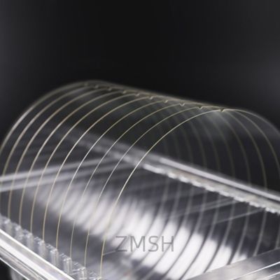
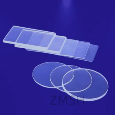
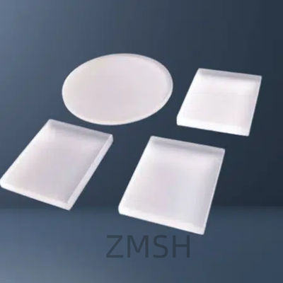
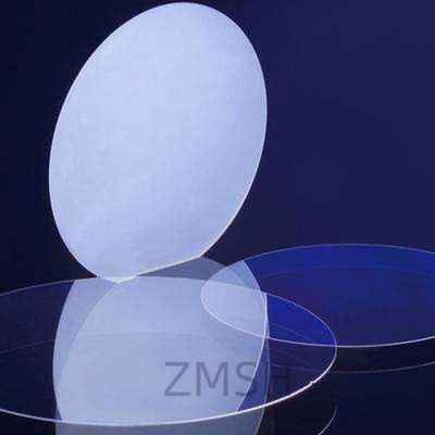
Quartz Wafer
Product Details:
| Place of Origin: | China |
| Brand Name: | ZMSH |
| Model Number: | Quartz Wafer |
Payment & Shipping Terms:
| Minimum Order Quantity: | 25 |
|---|---|
| Price: | 20USD |
| Packaging Details: | custom cartons |
| Delivery Time: | 2-4 weeks |
| Payment Terms: | T/T |
| Supply Ability: | By case |
|
Detail Information |
|||
| Diameter (inch): | 3/4/6/8/12 | Internal Transmittance: | >99.9% |
|---|---|---|---|
| Refractive Index: | 1.474698 | Total Transmittance: | >92% |
| TTV: | <3 | Flatness: | <15 |
Product Description
Introduction of Quartz Wafer
Quartz wafers are made from crystalline silicon dioxide (SiO₂). The unique properties of quartz make it an essential material in various high-tech industries.
Quartz wafers exhibit excellent characteristics such as high thermal resistance, superior light transmission at specific wavelengths, chemical inertness, and a low coefficient of thermal expansion. These features make them highly suitable for applications that require stability under extreme temperatures, resistance to harsh chemicals, and transparency in specific spectral ranges.
In industries such as semiconductor manufacturing, optics, and MEMS (Micro-Electro-Mechanical Systems), quartz wafers are widely used due to their ability to withstand high temperatures without deformation or degradation. They serve as substrates for thin-film deposition, microstructure etching, or the fabrication of precision components that demand high dimensional accuracy and thermal stability.
Manufacturing Principle of Quartz Wafer
-
Crystal Growth
Quartz boules are grown using natural or synthetic seed crystals through hydrothermal or flame fusion (Verneuil) methods. -
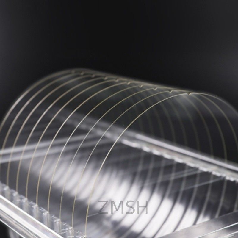
Ingot Slicing
Cylindrical ingots are sliced into wafers using diamond wire saws, ensuring thickness uniformity and minimal kerf loss. -
Lapping and Polishing
Wafers are lapped, etched, and then polished to achieve a mirror-smooth finish with low surface roughness (Ra < 1 nm for optical-grade wafers). -
Cleaning & Inspection
Ultrasonic or RCA cleaning removes particulates and metallic contaminants. Each wafer undergoes dimensional and surface flatness inspection.
Quartz Wafer Specifications
| Quartz Type | 4 | 6 | 8 | 12 |
|---|---|---|---|---|
| Size | ||||
| Diameter (inch) | 4 | 6 | 8 | 12 |
| Thickness (mm) | 0.05–2 | 0.25–5 | 0.3–5 | 0.4–5 |
| Diameter Tolerance (inch) | ±0.1 | ±0.1 | ±0.1 | ±0.1 |
| Thickness Tolerance (mm) | Customizable | Customizable | Customizable | Customizable |
| Optical Properties | ||||
| Refractive Index @365 nm | 1.474698 | 1.474698 | 1.474698 | 1.474698 |
| Refractive Index @546.1 nm | 1.460243 | 1.460243 | 1.460243 | 1.460243 |
| Refractive Index @1014 nm | 1.450423 | 1.450423 | 1.450423 | 1.450423 |
| Internal Transmittance (1250–1650 nm) | >99.9% | >99.9% | >99.9% | >99.9% |
| Total Transmittance (1250–1650 nm) | >92% | >92% | >92% | >92% |
| Machining Quality | ||||
| TTV (Total Thickness Variation, µm) | <3 | <3 | <3 | <3 |
| Flatness (µm) | ≤15 | ≤15 | ≤15 | ≤15 |
| Surface Roughness (nm) | ≤1 | ≤1 | ≤1 | ≤1 |
| Bow (µm) | <5 | <5 | <5 | <5 |
| Physical Properties | ||||
| Density (g/cm³) | 2.20 | 2.20 | 2.20 | 2.20 |
| Young's Modulus (GPa) | 74.20 | 74.20 | 74.20 | 74.20 |
| Mohs Hardness | 6–7 | 6–7 | 6–7 | 6–7 |
| Shear Modulus (GPa) | 31.22 | 31.22 | 31.22 | 31.22 |
| Poisson's Ratio | 0.17 | 0.17 | 0.17 | 0.17 |
| Compressive Strength (GPa) | 1.13 | 1.13 | 1.13 | 1.13 |
| Tensile Strength (MPa) | 49 | 49 | 49 | 49 |
| Dielectric Constant (1 MHz) | 3.75 | 3.75 | 3.75 | 3.75 |
| Thermal Properties | ||||
| Strain Point (10¹⁴.⁵ Pa·s) | 1000°C | 1000°C | 1000°C | 1000°C |
| Annealing Point (10¹³ Pa·s) | 1160°C | 1160°C | 1160°C | 1160°C |
| Softening Point (10⁷.⁶ Pa·s) | 1620°C | 1620°C | 1620°C | 1620°C |