


 |
GaN Gallium Nitride Wafer High Electron Mobility RF Devices Optoelectronics And LEDs
Product Details:
| Place of Origin: | China |
| Brand Name: | ZMSH |
| Model Number: | GaN Gallium Nitride Wafer |
Payment & Shipping Terms:
| Delivery Time: | 2-4 weeks |
|---|---|
| Payment Terms: | T/T |
|
Detail Information |
|||
| Dimension: | 1" Diameter Or 25.4 +/- 0.5 Mm | Thickness: | 350 +/- 50 Um |
|---|---|---|---|
| Primary Flat: | 12 +/- 1 Mm | Secondary Flat:: | 8 +/- 1 Mm |
| Orientation: | (0001) C-plane | Total Thickness Variation: | ≤ 40 Um |
| Bow: | 0 +/- 10 Um | Resistivity: | ~ 10-3 Ohm-cm |
| Carrier Concentration: | ~ 1019 Cm-3 | Carrier Mobility: | ~ 150 Cm2/V*s |
| Etch Pit Density: | < 5 X 10⁴ Cm-2 | Polishing: | Front Surface: RMS < 0.5 Nm, Epi Ready, Back Surface Ground. |
| High Light: | Optoelectronics Gallium Nitride Wafer,LEDs GaN Wafer,RF Devices Gallium Nitride Wafer |
||
Product Description
GaN Gallium Nitride Wafer High Electron Mobility RF Devices Optoelectronics and LEDs
GaN Gallium Nitride Wafer's abstract
Gallium Nitride (GaN) wafers have emerged as a pivotal technology in various industries, owing to their unique material properties. With a wide bandgap, high electron mobility, and exceptional thermal stability, GaN wafers find applications in power electronics, RF devices, optoelectronics, and more. This abstract explores the versatile applications of GaN wafers, from powering 5G communications to illuminating LEDs and advancing solar energy systems. The high-performance characteristics of GaN make it a cornerstone in the development of compact and efficient electronic devices, influencing sectors such as automotive electronics, aerospace, and renewable energy. As a driving force in technological innovation, GaN wafers continue to redefine possibilities across diverse industries, shaping the landscape of modern electronics and communication systems.
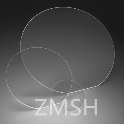
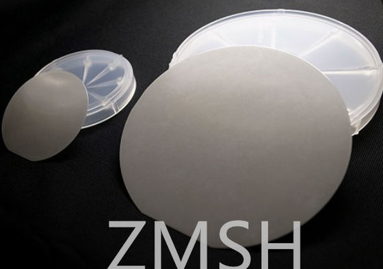
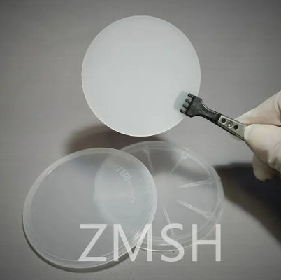
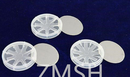
GaN Gallium Nitride Wafer's showcase
![]()
![]()
![]()
![]()
GaN Gallium Nitride Wafer's application
![]()
Gallium Nitride (GaN) wafers find a wide range of applications across multiple industries, leveraging their unique material properties for enhanced performance in electronic and optoelectronic devices. Here are some key applications of GaN wafers:
-
Power Electronics:
- GaN wafers are extensively used in power electronic devices such as transistors and diodes. Their high electron mobility and wide bandgap make them suitable for applications like power amplifiers, converters, and inverters in industries ranging from telecommunications to renewable energy systems.
-
RF (Radio Frequency) Devices:
- GaN wafers are employed in the development of high-frequency RF devices, including amplifiers and switches. The high electron mobility of GaN allows for efficient RF signal processing, making it valuable in applications such as radar systems, wireless communication, and satellite communication.
-
Optoelectronics and LEDs:
- GaN-based LEDs (Light-Emitting Diodes) are widely used in lighting applications, displays, and indicators. The ability of GaN to emit light in the blue and ultraviolet spectrum contributes to the production of white light in LEDs, making them crucial for energy-efficient lighting solutions.
-
UV (Ultraviolet) Optoelectronic Devices:
- GaN's transparency to ultraviolet light makes it suitable for UV optoelectronic applications. GaN wafers are used in the fabrication of UV sensors, sterilization equipment, and other devices where sensitivity to UV radiation is essential.
-
High-Electron-Mobility Transistors (HEMTs):
- GaN wafers serve as a key material for the development of HEMTs, which are high-performance transistors used in high-frequency and high-power applications. HEMTs based on GaN technology are employed in satellite communications, radar systems, and wireless infrastructure.
-
Wireless Communication (5G):
- The high-frequency capabilities of GaN make it a preferred material for the development of RF components in 5G communication systems. GaN-based amplifiers and transmitters play a crucial role in enabling the high data rates and low latency required for 5G networks.
-
Power Supplies and Converters:
- GaN wafers are utilized in the manufacturing of power supplies and converters, where high-efficiency and compact designs are essential. GaN-based power devices contribute to reducing power losses and improving the overall efficiency of electronic systems.
-
Automotive Electronics:
- GaN technology is finding increased use in automotive electronics, particularly in electric vehicles (EVs) and hybrid electric vehicles (HEVs). GaN-based power electronics enhance the efficiency of electric drivetrains, contributing to the advancement of sustainable transportation.
-
Solar Power Inverters:
- GaN wafers are employed in the development of power inverters for solar energy systems. The high efficiency and power handling capabilities of GaN devices contribute to optimizing the conversion of solar energy into usable electricity.
-
Advanced Radar Systems:
- GaN's ability to operate at high frequencies and withstand high-power levels makes it ideal for advanced radar systems. GaN-based devices enhance the performance of radar applications in defense, aerospace, and weather monitoring.
The diverse applications of GaN wafers underscore their significance in advancing technology across multiple sectors. The material's unique combination of high electron mobility, wide bandgap, and other beneficial properties positions GaN as a key enabler for the development of advanced electronic and optoelectronic devices.
GaN Gallium Nitride Wafer's data chart