


|
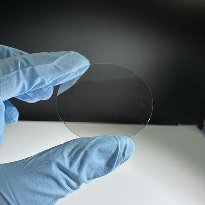
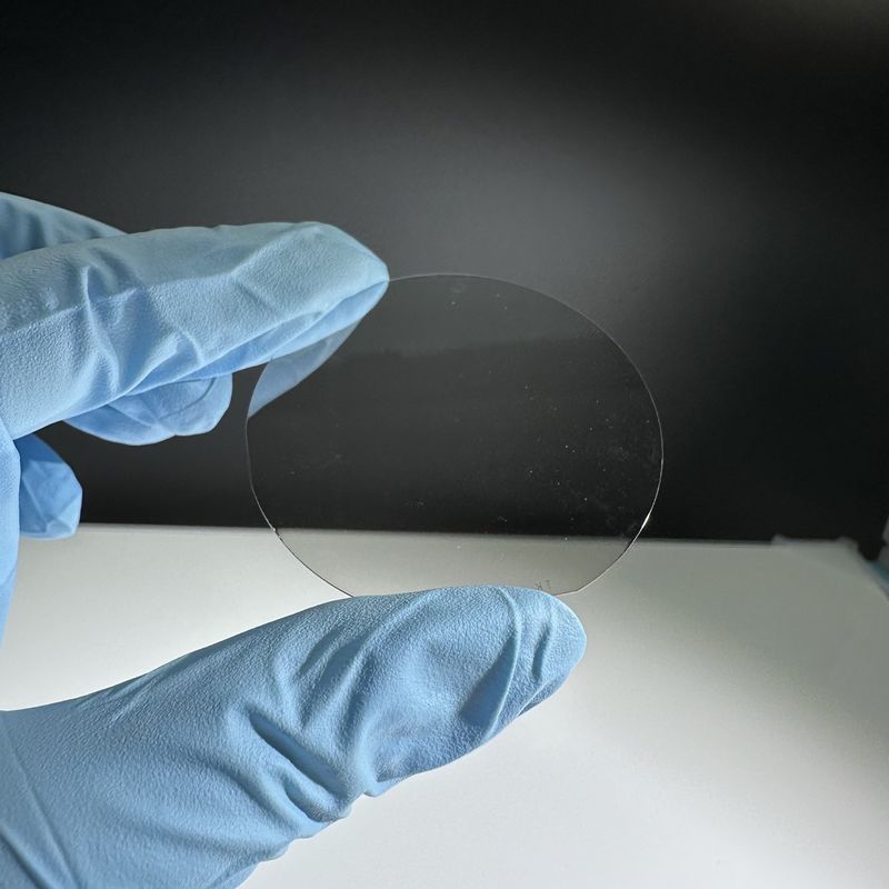
Semi Insulating Silicon Carbide Wafer SiC Substrate Orientation 0001 Bow/Warp ≤50um
Product Details:
| Place of Origin: | China |
| Brand Name: | ZMSH |
| Certification: | ROHS |
| Model Number: | Silicon Carbide |
Payment & Shipping Terms:
| Minimum Order Quantity: | 1 |
|---|---|
| Delivery Time: | 2 weeks |
| Payment Terms: | 100%T/T |
| Supply Ability: | 10000 |
|
Detail Information |
|||
| Resistivity: | High Resistivity | Diameter: | 2inch 3inch 4inch 6inch 8inch |
|---|---|---|---|
| Flatness: | Lambda/10 | Type: | 4H-Semi-insulting/ 6H-Semi-insulting |
| Conductivity: | High Conductivity | Particle: | Free/Low Particle |
| Surface Roughness: | ≤0.2nm | Impurity: | Free/Low Impurity |
| High Light: | High Temperature Silicon Carbide Wafer,Semi Insulating SiC Substrate,6inch SiC Substrate |
||
Product Description
Product Description:
ZMSH — Innovative Manufacturer and Supplier of SiC Substrate WafersAs the leading manufacturer and supplier of SiC (Silicon Carbide) substrate wafer, ZMSH not only offers the best price on the market for 2 inch and 3 inch Research grade Silicon Carbide substrate wafers, but also provides innovative solutions for electronic devices with high power and high frequency, light emitting diode (LED).
Light emitting diode (LED) is an energy-saving cold light source that uses semiconductor electrons and holes in combination with electronic components. The wide range of applications for LED lighting has been recognized in recent years due to its numerous advantages.
For customers looking for a reliable manufacturer and supplier of SiC substrate wafers, ZMSH is the one-stop solution to fulfill all their needs.
Features:
Silicon Carbide (SiC) single crystal has excellent thermal conductivity properties, high saturation electron mobility, and high voltage breakdown resistance.
It is suitable for preparing high frequency, high power, high temperature, and radiation-resistant electronic devices.
SiC single crystal has many excellent properties, such as high thermal conductivity, high saturated electron mobility, and strong anti-voltage breakdown. Suitable for preparation of high frequency, high power, high temperature and radiation-resistant electronic devices.
Technical Parameters:
Product Name: Silicon carbide substrate, Silicon carbide wafer, SiC wafer, SiC substrate
Growth method: MOCVD
Crystal Structure: 6H, 4H
Lattice Parameters: 6H(a=3.073 Å c=15.117 Å), 4H(a=3.076 Å c=10.053 Å )
Stacking Sequence: 6H: ABCACB, 4H: ABCB
Grade: Production Grade, Research Grade, Dummy Grade
Conductivity type: N-type or Semi-Insulating
Band-gap: 3.23 eV
Hardness: 9.2 (mohs)
Thermal Conductivity @300K: 3.2~4.9 W/ cm.K
Dielectric constants: e(11)=e(22)=9.66 e(33)=10.33
Resistivity:
- 4H-SiC-N: 0.015~0.028 Ω·cm,
- 6H-SiC-N: 0.02~0.1 Ω·cm,
- 4H/6H-SiC-SI: >1E7 Ω·cm
Packing: Class 100 clean bag, in class 1000 clean room
Applications:
Silicon Carbide Wafer (SiC wafer) is an ideal material to be used for automotive electronics, optoelectronic devices, and industrial applications. The SiC wafer is composed of 4H-N Type SiC substrate and Semi-Insulating SiC substrate.
In the automotive industry, SiC wafer can be applied to pump microprocessor, microcomputer, motor control, and other cars and buses electronic devices. For example, it can be used in the engine control, braking system, air bag systems, and body extended control. SiC wafers can be produced with different layers of different materials, which makes it useful for more then one function.
Additionally, the SiC wafer is widely utilized in the optoelectronic devices, such as lasers, detectors, LED, detectors, optical amplification, super-luminescent emitter, photodetectors, and other optoelectronic components. Moreover, in the industrial applications, the SiC wafer can be used for optical power generation, exchange, and transmission, including solar, light, and fault monitoring, and other fiber optic devices.
Support and Services:
We provide comprehensive technical support and service for Silicon Carbide Wafer. Our technical support team is comprised of experienced engineers and technicians, who are available to provide you with the assistance and advice you need.
We provide a range of services, including technical support, troubleshooting, installation, maintenance and repair. We can also provide custom solutions for any of your needs. Our technicians are well-versed in the latest technologies and can help you make the most out of your Silicon Carbide Wafer.
We have a wide network of partners and suppliers, so we can provide you with the best possible prices and support. We strive to provide you with the highest level of customer service, and we are committed to meeting your needs and exceeding your expectations.
If you have any questions or need any assistance, please don't hesitate to contact us. We look forward to helping you get the most out of your Silicon Carbide Wafer.
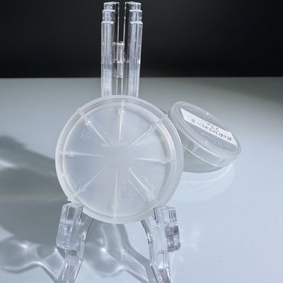
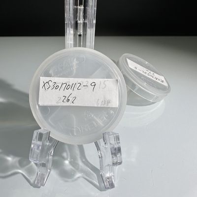
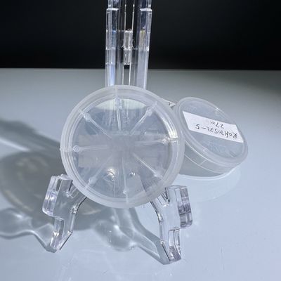
Packing and Shipping:
Silicon Carbide (SiC) Wafers are thin slices of semiconductor material primarily used for power electronics. To ensure the wafers are not damaged during shipping, it’s important to follow the proper packaging and shipping instructions.
Packaging
- Wafers must be shipped in an ESD safe package.
- Each wafer should be wrapped in ESD safe material such as an ESD foam or bubble wrap.
- The package should be sealed with ESD safe tape.
- The package should be labeled with the ESD safe symbol and "Fragile" sticker.
Shipping
- The package should be shipped using a reliable courier service.
- The package should be tracked to ensure it arrives at its destination safely.
- The package should be labeled with the proper shipping address and contact information.
![]()
![]()
![]()
FAQ:
- Q: What is Silicon Carbide Wafer?
- A: Silicon Carbide Wafer is a semiconductor material made from silicon and carbon atoms bonded together in a crystal lattice.
- Q: What is the brand name of Silicon Carbide Wafer?
- A: The brand name of Silicon Carbide Wafer is ZMSH.
- Q: What is the model number of Silicon Carbide Wafer?
- A: The model number of Silicon Carbide Wafer is Silicon Carbide.
- Q: Where is Silicon Carbide Wafer from?
- A: Silicon Carbide Wafer is from China.
- Q: What is the minimum order quantity of Silicon Carbide Wafer?
- A: The minimum order quantity of Silicon Carbide Wafer is 5.
- Q: How long is the delivery time of Silicon Carbide Wafer?
- A: The delivery time of Silicon Carbide Wafer is 2 weeks.
- Q: What is the payment terms of Silicon Carbide Wafer?
- A: The payment terms of Silicon Carbide Wafer is 100%T/T.
- Q: What is the supply ability of Silicon Carbide Wafer?
- A: The supply ability of Silicon Carbide Wafer is 100000.