


|
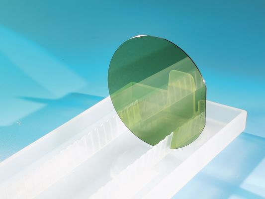
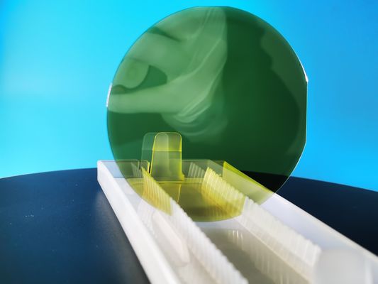
2inch 4inch 6inch 8inch Industrial Use Silicon Carbide Wafer With Surface Roughness ≤0.2nm
Product Details:
| Place of Origin: | China |
| Brand Name: | ZMSH |
| Certification: | ROHS |
| Model Number: | Silicon Carbide |
Payment & Shipping Terms:
| Minimum Order Quantity: | 5 |
|---|---|
| Delivery Time: | 2-4 weeks |
| Payment Terms: | 100%T/T |
| Supply Ability: | 100000 |
|
Detail Information |
|||
| Surface Finish: | Single/Double Side Polished | Surface Roughness: | ≤0.2nm |
|---|---|---|---|
| Conductivity: | High/Low Conductivity | Particle: | Free/Low Particle |
| Grade: | Production/ Research/ Dummy | Impurity: | Free/Low Impurity |
| Doped: | Silicon Doped/Un-doped/Zn Doped | Type: | 4H-N/ 6H-N/ 4H-Semi-insulting/ 6H-Semi-insulting |
| High Light: | Double Side Polished Silicon Carbide Substrate,Industrial Use Silicon Carbide Wafer,Silicon Carbide Wafer 8inch |
||
Product Description
Product Description:
ZMSH has become the leading manufacturer and supplier of SiC (Silicon Carbide) substrate wafers. For customers looking for excellent value, ZMSH offers the best current price on the market for 2 inch and 3 inch Research grade SiC substrate wafers.
SiC substrate wafers have a variety of applications in electronic device design, specifically for products involving high power and high frequency.
Furthermore, LED technology is a major consumer of SiC substrate wafers. LED stands for Light Emitting Diode, which is a type of semiconductor that combines electrons and holes to create an energy-efficient cold light source.
Features:
Silicon Carbide (SiC) single crystal has many outstanding properties, such as excellent thermal conductivity, high saturation electron mobility, and high voltage breakdown resistance. These properties make it the perfect material for preparing high frequency, high power, high temperature, and radiation-resistant electronic devices.
In addition, SiC single crystal has excellent thermal conductivity and strong voltage breakdown properties. It can easily withstand high temperature and radiation levels without deteriorating, making it the ideal choice for high-end electronic devices.
Moreover, the high electron mobility of SiC single crystal provides greater efficiency compared to other materials, allowing it to work longer with fewer interruptions. Thus, it is the perfect material for creating high performance, reliable electronics.
Technical Parameters:
Product Name: Silicon carbide substrate, Silicon carbide wafer, SiC wafer, SiC substrate
Growth method: MOCVD
Crystal Structure: 6H, 4H, 6H(a=3.073 Å c=15.117 Å), 4H(a=3.076 Å c=10.053 Å )
Stacking Sequence: 6H: ABCACB, 4H: ABCB
Grade: Production Grade, Research Grade, Dummy Grade
Conductivity type: N-type or Semi-Insulating
Band-gap: 3.23 eV
Hardness: 9.2(mohs)
Thermal Conductivity @300K: 3.2~4.9 W/ cm.K
Dielectric constants: e(11)=e(22)=9.66 e(33)=10.33
Resistivity: 4H-SiC-N: 0.015~0.028 Ω·cm, 6H-SiC-N: 0.02~0.1 Ω·cm, 4H/6H-SiC-SI: >1E7 Ω·cm
Packing: Class 100 clean bag, in class 1000 clean room.
Applications:
Silicon Carbide Wafer (SiC wafer) is an ideal option for automotive electronics, optoelectronic devices, and industrial applications. These wafers include both 4H-N Type SiC substrates and semi-insulating SiC substrates, which are both key components of various devices.
4H-N type SiC substrates provide superior properties such as a wide band gap, which allows for very efficient switching in power electronics. Additionally, they are highly resistant to mechanical wear and chemical oxidation, making them ideal for high-temperature, low-loss devices.
Semi-insulating SiC substrates also provide excellent properties, such as high stability and thermal resistance. Their ability to remain stable in high-power devices makes them ideal for various optoelectronic applications. Furthermore, they can also be used as bonded wafers, which are important components in high-performance microelectronic devices.
These features of SiC wafer make them suitable for various applications, especially in the automotive, optoelectronic, and industrial sectors. SiC wafers are an essential part of today’s technology and are continuing to become increasingly popular in a variety of industries.
Support and Services:
We offer comprehensive technical support and services for Silicon Carbide Wafer. Our team of experts are available to provide guidance on product selection, answer any technical questions, and help with design and implementation of your project.
Our knowledgeable technical support team is available to answer any questions or concerns you may have about Silicon Carbide Wafer. We provide in-depth product information, application support, and troubleshooting assistance.
We can help you select the best Silicon Carbide Wafer product for your application. Our team of experts can provide recommendations, samples, and support to ensure you make the perfect choice.
Our team of experienced engineers can help you design and implement the perfect Silicon Carbide Wafer solution. We can provide detailed drawings, simulations, and support to ensure your project is successful.
Packing and Shipping:
Silicon carbide wafers are fragile and require special handling and protection when shipping. The following procedures should be followed to ensure safe delivery to the customer.
- The wafers should be placed in static-dissipative packaging with anti-static foam.
- The wafers should be sealed in a moisture barrier bag to protect them from environmental contaminants.
- The packaging should be sealed in a box with cushioning material to protect against shock and vibration.
- The box should be labeled with the following information: the customer's address, the contents of the package, and the weight of the package.
- The package should be shipped with an appropriate carrier and be insured for the full value of the contents.
FAQ:
Q1: What is Silicon Carbide Wafer?A1: Silicon Carbide Wafer is a wafer made from silicon carbide material, which is a semiconductor material with a wide bandgap and high thermal conductivity. It is suitable for power electronics and other high-temperature applications.
Q2: What is the brand name of this product?
A2: The brand name of this product is ZMSH.
Q3: What is the model number of this product?
A3: The model number of this product is Silicon Carbide.
Q4: What is the minimum order quantity?
A4: The minimum order quantity is 5.
Q5: How long is the delivery time?
A5: The delivery time is 2 weeks.