


|
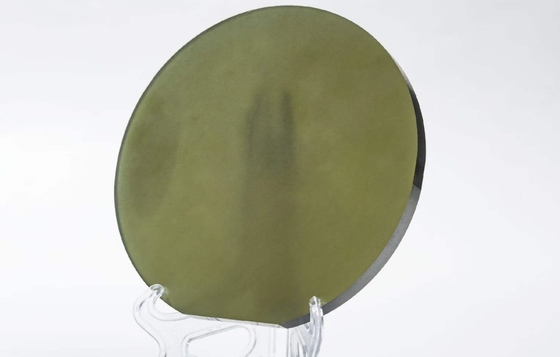
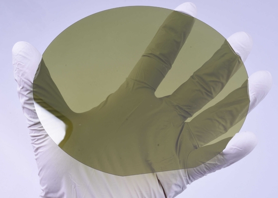
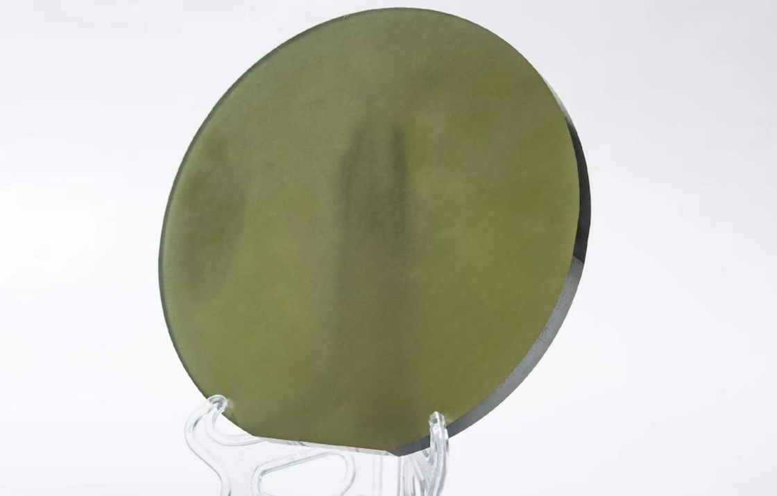
Monocrystalline SiC Silicon Carbide Wafer Substrate Dummy Grade Dia153mm 156mm 159mm
Product Details:
| Place of Origin: | CHINA |
| Brand Name: | ZMKJ |
| Certification: | ROHS |
| Model Number: | 6Inch SiC substrate dummy |
Payment & Shipping Terms:
| Minimum Order Quantity: | 1pcs |
|---|---|
| Price: | by case |
| Packaging Details: | single wafer package in 100-grade cleaning room |
| Delivery Time: | 3-6weeks |
| Payment Terms: | T/T, Western Union, MoneyGram |
| Supply Ability: | 1-50pcs/month |
|
Detail Information |
|||
| Material: | Monocrystalline Silicon Carbide | Hardness: | 9.4 |
|---|---|---|---|
| Application: | MOS And SBD | Tolerance: | ±0.1mm |
| Type: | 4h-n 4h-semi 6h-semi | Diameter: | 150-160mm |
| Thickness: | 0.1-15mm | Resistivity: | 0.015~0 028 O-cm |
| High Light: | Monocrystalline SiC Silicon Carbide Wafer,Dummy Grade Silicon Carbide Wafer,Monocrystalline SiC Wafer |
||
Product Description
6Inch Dia153mm 156mm 159mm Monocrystalline SiC Silicon Carbide Wafer Substrate Dummy Grade
About Silicon Carbide (SiC)Crystal
Silicon carbide substrate can be divided into conductive type and semi-insulating type according to resistivity. Conductive silicon carbide devices are mainly used in electric vehicles, photovoltaic power generation, rail transit, data centers, charging and other infrastructure. The electric vehicle industry has a huge demand for conductive silicon carbide substrates, and at present, Tesla, BYD, NIO, Xiaopeng and other new energy vehicle companies have planned to use silicon carbide discrete devices or modules.
Semi-insulated silicon carbide devices are mainly used in 5G communications, vehicle communications, national defense applications, data transmission, aerospace and other fields. By growing the gallium nitride epitaxial layer on the semi-insulated silicon carbide substrate, the silicon-based gallium nitride epitaxial wafer can be further made into microwave RF devices, which are mainly used in the RF field, such as power amplifiers in 5G communication and radio detectors in national defense.
The manufacturing of silicon carbide substrate products involves equipment development, raw material synthesis, crystal growth, crystal cutting, wafer processing, cleaning and testing, and many other links. In terms of raw materials, Songshan Boron industry provides silicon carbide raw materials for the market, and has achieved small batch sales. The third generation semiconductor materials represented by silicon carbide play a key role in modern industry, with the acceleration of penetration of new energy vehicles and photovoltaic applications, the demand for silicon carbide substrate is about to usher in an inflection point
1. Description
|
Item |
Specifications |
|
|---|---|---|
|
Polytype |
4H -SiC |
6H- SiC |
|
Diameter |
2 inch | 3 inch | 4 inch | 6inch |
2 inch | 3 inch | 4 inch | 6inch |
|
Thickness |
330 μm ~ 350 μm |
330 μm ~ 350 μm |
|
Conductivity |
N – type / Semi-insulating |
N – type / Semi-insulating |
|
Dopant |
N2 ( Nitrogen )V ( Vanadium ) |
N2 ( Nitrogen ) V ( Vanadium ) |
|
Orientation |
On axis <0001> |
On axis <0001> |
|
Resistivity |
0.015 ~ 0.03 ohm-cm |
0.02 ~ 0.1 ohm-cm |
|
Micropipe Density(MPD) |
≤10/cm2 ~ ≤1/cm2 |
≤10/cm2 ~ ≤1/cm2 |
|
TTV |
≤ 15 μm |
≤ 15 μm |
|
Bow / Warp |
≤25 μm |
≤25 μm |
|
Surface |
DSP/SSP |
DSP/SSP |
|
Grade |
Production / Research grade |
Production / Research grade |
|
Crystal Stacking Sequence |
ABCB |
ABCABC |
|
Lattice parameter |
a=3.076A , c=10.053A |
a=3.073A , c=15.117A |
|
Eg/eV(Band-gap) |
3.27 eV |
3.02 eV |
|
ε(Dielectric Constant) |
9.6 |
9.66 |
|
Refraction Index |
n0 =2.719 ne =2.777 |
n0 =2.707 , ne =2.755 |
Application of SiC in power device industry
Compared with silicon devices, silicon carbide (SiC) power devices can effectively achieve high efficiency, miniaturization and light weight of power electronic systems. The energy loss of SiC power devices is only 50% of Si devices, and the heat generation is only 50% of silicon devices, SiC also has a higher current density. At the same power level, the volume of SiC power modules is significantly smaller than that of silicon power modules. Taking the intelligent power module IPM as an example, using SiC power devices, the module volume can be reduced to 1/3 to 2/3 of silicon power modules.
There are three types of SiC power diodes: Schottky diodes (SBD), PIN diodes and junction barrier controlled Schottky diodes (JBS). Because of the Schottky barrier, SBD has a lower junction barrier height, so SBD has the advantage of low forward voltage. The emergence of SiC SBD has enlarged the application range of SBD from 250V to 1200V. In addition, its characteristics at high temperature are good, the reverse leakage current not increases from room temperature to 175 ° C. In the application field of rectifiers above 3kV, SiC PiN and SiC JBS diodes have received much attention due to their higher breakdown voltage, faster switching speed, smaller size and lighter weight than silicon rectifiers.
SiC power MOSFET devices have ideal gate resistance, high-speed switching performance, low on-resistance, and high stability. It is the preferred device in the field of power devices below 300V. There are reports that a silicon carbide MOSFET with a blocking voltage of 10kV has been successfully developed. Researchers believe that SiC MOSFETs will occupy an advantageous position in the field of 3kV - 5kV.
SiC Insulated Gate Bipolar Transistors (SiC BJT, SiC IGBT) and SiC Thyristor (SiC Thyristor), SiC P-type IGBT devices with a blocking voltage of 12 kV have good forward current capability. Compared with Si bipolar transistors, SiC bipolar transistors have 20-50 times lower switching losses and lower turn-on voltage drop. SiC BJT is mainly divided into epitaxial emitter BJT and ion implantation emitter BJT, the typical current gain is between 10-50.
About ZMKJ Company
ZMKJ can provides high quality single crystal SiC wafer ( Silicon Carbide ) to electronic and optoelectronic industry . SiC wafer is a next generation semiconductor material , with unique electrical properties and excellent thermal properties , compared to silicon wafer and GaAs wafer , SiC wafer is more suitable for high temperature and high power device application . SiC wafer can be supplied in diameter 2-6 inch , both 4H and 6H SiC , N-type , Nitrogen doped , and semi-insulating type available . Please contact us for more product information .
1--What size are SiC wafers? We have 2inch 3inch 4inch 6inch 8inch in stock now.
2--How much does a SiC wafer cost? It will depend on your demands
3--How thick are silicon carbide wafers? Generally speaking, the SiC wafer thickness is 0.35 and 0.5mm. We also have accept customized.
4--What is the use of SiC wafer? SBD, MOS, and others
FAQ:
Q: What's the way of shipping and cost?
A:(1) We accept DHL, Fedex, EMS etc.
(2) it is fine If you have your own express account ,If not,we could help you ship them and
Freight is in accordance with the actual settlement.
Q: How to pay?
A: T/T 100% deposit before delivery.
Q: What's your MOQ?
A: (1) For inventory, the MOQ is 1pcs. if 2-5pcs it's better.
(2) For customized commen products, the MOQ is 10pcs up.
Q: What's the delivery time?
A: (1) For the standard products
For inventory: the delivery is 5 workdays after you place the order.
For customized products: the delivery is 2 -4 weeks after you order contact.
Q: Do you have standard products?
A: Our standard products in stock. as like substrates 4inch 0.35mm.