


 |
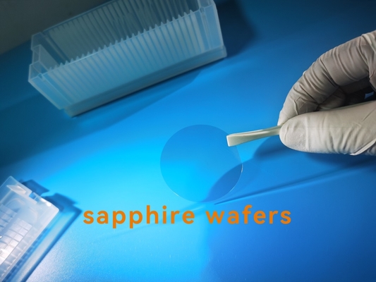
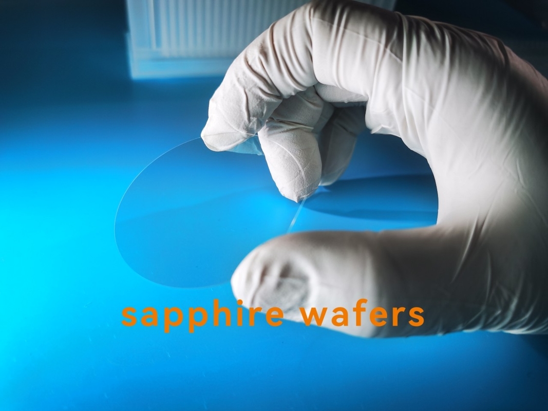
2inch 4inch 6inch Sapphire Wafer Substrate Single Crystal C Miscut A Degree M Plane
Product Details:
| Place of Origin: | China |
| Brand Name: | zmkj |
| Certification: | ROHS |
| Model Number: | C-axis M-axis carrier sapphire wafer |
Payment & Shipping Terms:
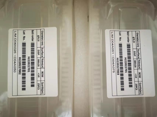
| Minimum Order Quantity: | 25pcs |
|---|---|
| Price: | by case |
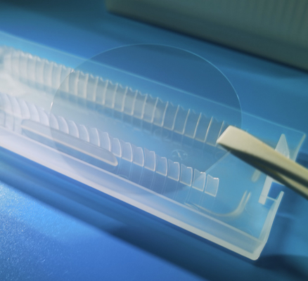
| Packaging Details: | in 25pcs cassette wafer box under 100grade cleaning room |
| Delivery Time: | 2 weeks |
| Payment Terms: | T/T, Western Union, MoneyGram |
| Supply Ability: | 1000pcs per month |
|
Detail Information |
|||
| Material: | Sapphire Single Crystal Al2O3 99.999% | Orientation: | C-AXIS/A-AXIS/M-AXIS/M-AXIS |
|---|---|---|---|
| Surface: | Ssp Or Dsp | Thickness: | 0.1mm 0.25mm 0.3mm 0.43mm 0.7mm 1.0mm |
| Application: | Carrier Substrate Windows | Growth Method: | Ky |
| TTV: | <3um | Size: | 2inch/4inch/6inch/8inch/12inch |
| High Light: | Single Crystal Sapphire Wafer,6inch Sapphire Wafer,C Miscut Sapphire Substrate |
||
Product Description
2inch 4inch 6inch Sapphire Wafer Substrate Single Crystal C Miscut A Degree M Plane
TTV<3um 4.125inch/6inch/6.125inch/dia159mm R-axis sapphire Carrier wafers
About synthetic sapphire crystal
The Kyropoulos process (KY process) for sapphire crystal growth is currently used by many companies in China to produce sapphire for the electronics and optics industries.
High-purity, aluminum oxide is melted in a crucible at over 2100 degrees Celsius. Typically the crucible is made of tungsten or molybdenum. A precisely oriented seed crystal is dipped into the molten alumina. The seed crystal is slowly pulled upwards and may be rotated simultaneously. By precisely controlling the temperature gradients, rate of pulling, and rate of temperature decrease, it is possible to produce a large, single-crystal, roughly cylindrical ingot from the melt.
After single crystal sapphire boules are grown, they are core-drilled into cylindrical rods, The rods are sliced up into the desired window thickness and finally polished to the desired surface finish.
![]()
Use as substrate for semiconducting circuits
Thin sapphire wafers were the first successful use of an insulating substrate upon which to deposit silicon to make the integrated circuits known as silicon on sapphire or "SOS", Besides its excellent electrical insulating properties, sapphire has high thermal conductivity. CMOS chips on sapphire are especially useful for high-power radio-frequency (RF) applications such as those found in cellular telephones, public-safety band radios, and satellite communication systems.
Wafers of single-crystal sapphire are also used in the semiconductor industry as substrates for the growth of devices based on gallium nitride (GaN). The use of sapphire significantly reduces the cost, because it has about one-seventh the cost of germanium. Gallium nitride on sapphire is commonly used in blue light-emitting diodes (LEDs).
Used as a window material
Synthetic sapphire (sometimes referred to as sapphire glass) is commonly used as a window material, because it is both highly transparent to wavelengths of light between 150 nm (UV) and 5500 nm (IR) (the visible spectrum extends about 380 nm to 750 nm, and extraordinarily scratch-resistant. The key benefits of sapphire windows are:
* Very wide optical transmission band from UV to near-infrared
* Significantly stronger than other optical materials or glass windows
* Highly resistant to scratching and abrasion (9 on the Mohs scale of mineral hardness scale, the 3rd hardest natural substance next to moissanite and diamonds)
* Extremely high melting temperature (2030 °C)
CATALOGU & Stcok List
|
Standard wafer 2 inch C-plane sapphire wafer SSP/DSP
3 inch C-plane sapphire wafer SSP/DSP 4 inch C-plane sapphire wafer SSP/DSP 6 inch C-plane sapphire wafer SSP/DSP |
Special Cut
A-plane (1120) sapphire wafer R-plane (1102) sapphire wafer M-plane (1010) sapphire wafer N-plane (1123) sapphire wafer C-axis with a 0.5°~ 4° offcut, toward A-axis or M-axis Other customized orientation |
|
Customized Size
10*10mm sapphire wafer 20*20mm sapphire wafer Ultra thin (100um) sapphire wafer 8 inch sapphire wafer |
Patterned Sapphire Substrate (PSS)
2 inch C-plane PSS 4 inch C-plane PSS |
| 2inch |
DSP C-AXIS 0.1mm/ 0.175mm/0.2mm/0.3mm/0.4mm/0.5mm/1.0mmt SSP C-axis 0.2/0.43mm (DSP&SSP) A-axis/M-axis/R-axis 0.43mm
|
| 3inch |
DSP/ SSP C-axis 0.43mm/0.5mm
|
| 4Inch |
dsp c-axis 0.4mm/ 0.5mm/1.0mm ssp c-axis 0.5mm/0.65mm/1.0mmt
|
| 6inch |
ssp c-axis 1.0mm/1.3mmm
dsp c-axis 0.65mm/ 0.8mm/1.0mmt
|
![]()
![]()
![]()
![]()