


|
Square SiC Windows Silicon Carbide Substrate 2inch 4inch 6inch 8inch
Product Details:
| Place of Origin: | China |
| Brand Name: | ZMKJ |
| Certification: | ROHS |
| Model Number: | 10x10x0.5mmt |
Payment & Shipping Terms:
| Minimum Order Quantity: | 1pcs |
|---|---|
| Price: | by case |
| Packaging Details: | single wafer package in 100-grade cleaning room |
| Delivery Time: | 1-6weeks |
| Payment Terms: | T/T, Western Union, MoneyGram |
| Supply Ability: | 1-50pcs/month |
|
Detail Information |
|||
| Material: | SiC Single Crystal 4H-N Type | Grade: | Zero, Research, And Dunmy Grade |
|---|---|---|---|
| Thicnkss: | 0.1 0.2 0.3 0.35 0.43 0.5 | Application: | New Energy Vehicles, 5G Communications |
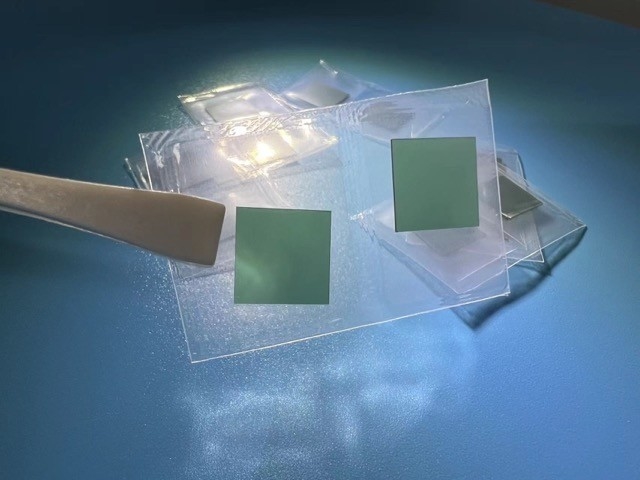
| Diameter: | 2-8inch Or 10x10mmt, 5x10mmt: | Color: | Green Tea |
| High Light: | 4inch Silicon Carbide Wafer,Silicon Carbide Window Substrate,Square SiC Wafer |
||
Product Description
Silicon carbide wafer optical 1/2/3 inch SIC wafer for sale Sic Plate Silicon Wafer Flat Orientation Enterprises for Sale 4inch 6inch seed sic wafer 1.0mm Thickness 4h-N SIC Silicon Carbide Wafer For seed growth 6H-N/6H-Semi 4H HPSI 5*10mmt 10x10mmt 5*5mm polished Silicon Carbide sic substrate chips Wafer
About Silicon Carbide (SiC)Crystal
Silicon carbide (SiC), or carborundum, is a semiconductor containing silicon and carbon with the chemical formula SiC. SiC is used in semiconductor electronics devices operating at high temperatures, high voltages, or both. SiC is also one of the important LED components, it is a popular substrate for growing GaN devices, and it also serves as a heat spreader in high-power LEDs.
|
Property
|
4H-SiC, Single Crystal
|
6H-SiC, Single Crystal
|
|
Lattice Parameters
|
a=3.076 Å c=10.053 Å
|
a=3.073 Å c=15.117 Å
|
|
Stacking Sequence
|
ABCB
|
ABCACB
|
|
Mohs Hardness
|
≈9.2
|
≈9.2
|
|
Density
|
3.21 g/cm3
|
3.21 g/cm3
|
|
Therm. Expansion Coefficient
|
4-5×10⁻⁶/K
|
4-5×10⁻⁶/K
|
|
Refraction Index @750nm
|
no = 2.61
ne = 2.66 |
no = 2.60
ne = 2.65 |
|
Dielectric Constant
|
c~9.66
|
c~9.66
|
|
Thermal Conductivity (N-type, 0.02 ohm.cm)
|
a~4.2 W/cm·K@298K
c~3.7 W/cm·K@298K |
|
|
Thermal Conductivity (Semi-insulating)
|
a~4.9 W/cm·K@298K
c~3.9 W/cm·K@298K |
a~4.6 W/cm·K@298K
c~3.2 W/cm·K@298K |
|
Band-gap
|
3.23 eV
|
3.02 eV
|
|
Break-Down Electrical Field
|
3-5×10⁶V/cm
|
3-5×10⁶V/cm
|
|
Saturation Drift Velocity
|
2.0×10⁵m/s
|
2.0×10⁵m/s
|
High purity 4inch diameter Silicon Carbide (SiC) Substrate Specification
| 2inch diameter Silicon Carbide (SiC) Substrate Specification | ||||||||||
| Grade | Zero MPD Grade | Production Grade | Research Grade | Dummy Grade | ||||||
| Diameter | 50.8 mm±0.2mm | |||||||||
| Thickness | 330 μm±25μm or 430±25um | |||||||||
| Wafer Orientation | Off axis : 4.0° toward <1120> ±0.5° for 4H-N/4H-SI On axis : <0001>±0.5° for 6H-N/6H-SI/4H-N/4H-SI | |||||||||
| Micropipe Density | ≤0 cm-2 | ≤5 cm-2 | ≤15 cm-2 | ≤100 cm-2 | ||||||
| Resistivity | 4H-N | 0.015~0.028 Ω•cm | ||||||||
| 6H-N | 0.02~0.1 Ω•cm | |||||||||
| 4/6H-SI | ≥1E5 Ω·cm | |||||||||
| Primary Flat | {10-10}±5.0° | |||||||||
| Primary Flat Length | 18.5 mm±2.0 mm | |||||||||
| Secondary Flat Length | 10.0mm±2.0 mm | |||||||||
| Secondary Flat Orientation | Silicon face up: 90° CW. from Prime flat ±5.0° | |||||||||
| Edge exclusion | 1 mm | |||||||||
| TTV/Bow /Warp | ≤10μm /≤10μm /≤15μm | |||||||||
| Roughness | Polish Ra≤1 nm | |||||||||
| CMP Ra≤0.5 nm | ||||||||||
| Cracks by high intensity light | None | 1 allowed, ≤2 mm | Cumulative length ≤ 10mm, single length≤2mm | |||||||
| Hex Plates by high intensity light | Cumulative area ≤1% | Cumulative area ≤1% | Cumulative area ≤3% | |||||||
| Polytype Areas by high intensity light | None | Cumulative area ≤2% | Cumulative area ≤5% | |||||||
| Scratches by high intensity light | 3 scratches to 1×wafer diameter cumulative length | 5 scratches to 1×wafer diameter cumulative length | 5 scratches to 1×wafer diameter cumulative length | |||||||
| edge chip | None | 3 allowed, ≤0.5 mm each | 5 allowed, ≤1 mm each | |||||||
![]()
![]()
![]()
![]()
SiC Applications
Silicon carbide (SiC) crystals have unique physical and electronic properties. Silicon Carbide based devices have been used for short wavelength optoelectronic, high temperature, radiation resistant applications. The high-power and high-frequency electronic devices made with SiC are superior to Si and GaAs-based devices. Below are some popular applications of SiC substrates.
Other products
8inch SiC wafer dummy grade 2inch SiC wafer
![]()
![]()
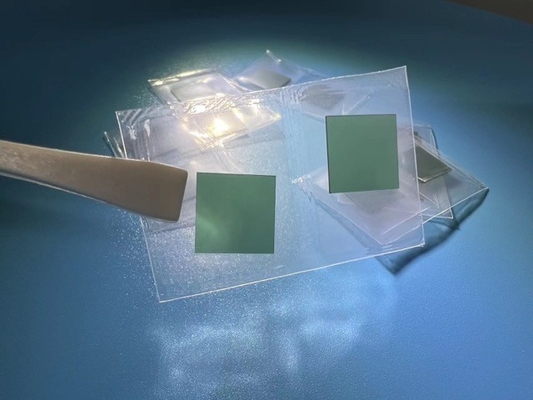
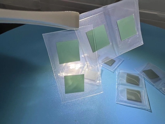
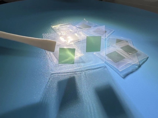
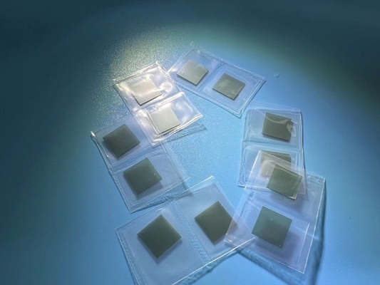
Packaging – Logistics
We are concerned with each detail of the package, cleaning, anti-static, and shock treatment.
According to the quantity and shape of the product, we will take a different packaging process! Almost by single wafer cassettes or 25pcs cassettes in the 100-grade cleaning room.
![]()