


 |
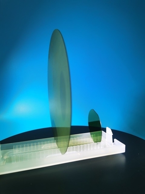
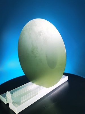
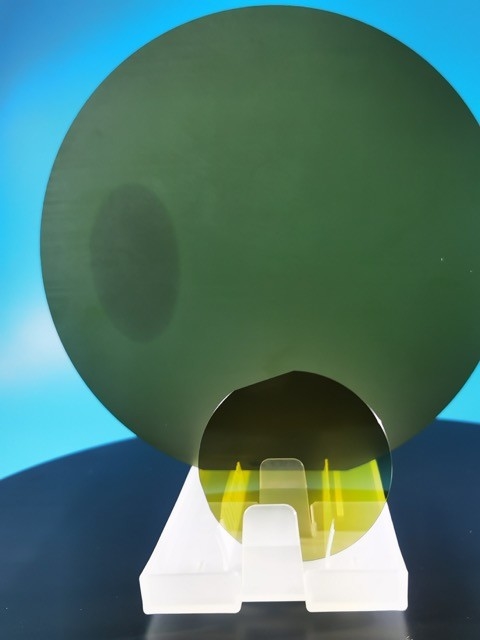
Polishing Silicon Carbide Ingot Substrate SiC Chip Semiconductor 8inch 200mm
Product Details:
| Place of Origin: | CHINA |
| Brand Name: | ZMKJ |
| Certification: | ROHS |
| Model Number: | 8inch sic wafers 4h-n |
Payment & Shipping Terms:
| Minimum Order Quantity: | 1pcs |
|---|---|
| Price: | by case |
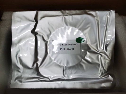
| Packaging Details: | single wafer package in 100-grade cleaning room |
| Delivery Time: | 4-6weeks |
| Payment Terms: | T/T, Western Union, MoneyGram |
| Supply Ability: | 1-50pcs/month |
|
Detail Information |
|||
| Material: | SiC Single Crystal | Grade: | Dummy Grade |
|---|---|---|---|
| Thicnkss: | 0.35mm 0.5mm | Suraface: | Double Side Polished |
| Application: | Device Maker Polishing Test | Diameter: | 200±0.5mm |
| MOQ: | 1 | Delivery Date: | 1-5 Piece Need One Week More Quantity Need 30 Days |
| High Light: | Polishing Silicon Carbide Ingot Substrate,200mm SiC Single Crystal,Silicon Carbide Wafer Semiconductor |
||
Product Description
SiC Substrate/Wafers (150mm, 200mm) Silicon Carbide Ceramic Excellent CorrosionSingle crystal single side polished silicon wafer sic wafer polishing wafer manufacturer Silicon Carbide SiC Wafer4H-N SIC ingots/200mm SiC Wafers 200mm SiC Wafers
About Silicon Carbide (SiC)Crystal
Silicon carbide (SiC), also known as carborundum, is a semiconductor containing silicon and carbon with chemical formula SiC. SiC is used in semiconductor electronics devices that operate at high temperatures or high voltages, or both.SiC is also one of the important LED components, it is a popular substrate for growing GaN devices, and it also serves as a heat spreader in high-power LEDs.
| Property | 4H-SiC, Single Crystal | 6H-SiC, Single Crystal |
| Lattice Parameters | a=3.076 Å c=10.053 Å | a=3.073 Å c=15.117 Å |
| Stacking Sequence | ABCB | ABCACB |
| Mohs Hardness | ≈9.2 | ≈9.2 |
| Density | 3.21 g/cm3 | 3.21 g/cm3 |
| Therm. Expansion Coefficient | 4-5×10⁻⁶/K | 4-5×10⁻⁶/K |
| Refraction Index @750nm |
no = 2.61 ne = 2.66 |
no = 2.60 ne = 2.65 |
| Dielectric Constant | c~9.66 | c~9.66 |
| Thermal Conductivity (N-type, 0.02 ohm.cm) |
a~4.2 W/cm·K@298K c~3.7 W/cm·K@298K |
|
| Thermal Conductivity (Semi-insulating) |
a~4.9 W/cm·K@298K c~3.9 W/cm·K@298K |
a~4.6 W/cm·K@298K c~3.2 W/cm·K@298K |
| Band-gap | 3.23 eV | 3.02 eV |
| Break-Down Electrical Field | 3-5×10⁶V/cm | 3-5×10⁶V/cm |
| Saturation Drift Velocity | 2.0×10⁵m/s | 2.0×10⁵m/s |
1) The preparation of high-quality 200mm 4H-SiC seed crystals;
2) Large size temperature field non-uniformity and nucleation process control;
3) The transport efficiency and evolution of gaseous components in large size crystal growth systems;
4) Crystal cracking and defect proliferation caused by large size thermal stress increase.
To overcome these challenges and obtain high quality 200mm SiC wafers,solutions are proposed:
In terms of 200mm seed crystal preparation, appropriate temperature field, flow field, and expanding assemblwere studied and designed to take into account crystal quality and expanding size; Starting with a 150mm SiCseed crystal, carry out seed crystal iteration to gradually expand the SiC crystal size until it reaches 200mm;Throuch multiple crystal growth and processing, gradually optimize the crystal quality in the crystal expandingarea, and improve the quality of 200mm seed crystals.
n terms of 200mm conductive crvstal and substrate preparation. research has optimized the temperature fieland flow field design for large size crystal growth, conduct 200mm conductive SiC crystal growth, and controldoping uniformity. After rough processing and shaping of the crystal, an 8-inch electrically conductive 4H-SiCingot with a standard diameter was obtained. After cutting, grinding, polishing, processing to obtain SiC 200mmwafers with a thickness of 525um or so.
![]()
![]()
About ZMKJ Company
ZMKJ can provides high quality single crystal SiC wafer ( Silicon Carbide ) to electronic and optoelectronic industry . SiC wafer is a next generation semiconductor material , with unique electrical properties and excellent thermal properties , compared to silicon wafer and GaAs wafer , SiC wafer is more suitable for high temperature and high power device application . SiC wafer can be supplied in diameter 2-6 inch , both 4H and 6H SiC , N-type , Nitrogen doped , and semi-insulating type available . Please contact us for more product information .
FAQ:
Q: What's the way of shipping and cost?
A:(1) We accept DHL, Fedex, EMS etc.
(2) it is fine If you have your own express account ,If not,we could help you ship them and
Freight is in accordance with the actual settlement.
Q: How to pay?
A: T/T 100% deposit before delivery.
Q: What's your MOQ?
A: (1) For inventory, the MOQ is 1pcs. if 2-5pcs it's better.
(2) For customized commen products, the MOQ is 10pcs up.
Q: What's the delivery time?
A: (1) For the standard products
For inventory: the delivery is 5 workdays after you place the order.
For customized products: the delivery is 2 -4 weeks after you order contact.
Q: Do you have standard products?
A: Our standard products in stock. as like substrates 4inch 0.35mm.