

 |
High Purity Silicon Carbide Wafer Prime/Dummy/Ultra Grade 4H-Semi SiC Wafers For 5G Device
Product Details:
| Place of Origin: | CHINA |
| Brand Name: | ZMKJ |
| Model Number: | 4inch high purity |
Payment & Shipping Terms:
| Minimum Order Quantity: | 1pcs |
|---|---|
| Price: | 1000-2000usd/pcs by FOB |
| Packaging Details: | single wafer package in 100-grade cleaning room |
| Delivery Time: | 1-6weeks |
| Payment Terms: | T/T, Western Union, MoneyGram |
| Supply Ability: | 1-50pcs/month |
|
Detail Information |
|||
| Material: | SiC High Purity Single Crystal 4H-semi Type | Grade: | Dummy / Research /Production Grade |
|---|---|---|---|
| Thicnkss: | 500um | Suraface: | CMP/MP |
| Application: | 5G Device | Diameter: | 100±0.3mm |
| Highlight: | silicon carbide substrate,sic wafer |
||
Product Description
High purity 4H-N 4inch 6inch dia 150mm silicon carbide single crystal (sic) substrates wafers, sic crystal ingots sic semiconductor substrates,Silicon Carbide crystal Wafer/ Customzied as-cut sic wafers
About Silicon Carbide (SiC)Crystal
Silicon carbide (SiC), also known as carborundum, is a semiconductor containing silicon and carbon with chemical formula SiC. SiC is used in semiconductor electronics devices that operate at high temperatures or high voltages, or both.SiC is also one of the important LED components, it is a popular substrate for growing GaN devices, and it also serves as a heat spreader in high-power LEDs.
PROPERTIES of 4H-SiC Single Crystal
- Lattice Parameters: a=3.073Å c=10.053Å
- Stacking Sequence: ABCB
- Mohs Hardness: ≈9.2
- Density: 3.21 g/cm3
- Therm. Expansion Coefficient: 4-5×10⁻⁶/K
- Refraction Index: no= 2.61 ne= 2.66
- Dielectric Constant: 9.6
- Thermal Conductivity: a~4.2 W/cm·K@298K
- (N-type, 0.02 ohm.cm) c~3.7 W/cm·K@298K
- Thermal Conductivity: a~4.9 W/cm·K@298K
- (Semi-insulating) c~3.9 W/cm·K@298K
- Band-gap: 3.23 eV Band-gap: 3.02 eV
- Break-Down Electrical Field: 3-5×10 6V/m
- Saturation Drift Velocity: 2.0×10⁵m/
![]()
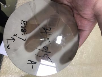
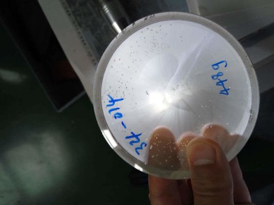
High purity 4inch diameter Silicon Carbide (SiC) Substrate Specification
4 inch Diameter High Purity 4H Silicon Carbide Substrate Specifications
|
SUBSTRATE PROPERTY |
Production Grade |
Research Grade |
Dummy Grade |
|
Diameter |
100.0 mm+0.0/-0.5 mm |
||
|
Surface Orientation |
{0001} ±0.2° |
||
|
Primary Flat Orientation |
<11-20> ± 5.0 ̊ |
||
|
Secondary Flat Orientation |
90.0 ̊ CW from Primary ± 5.0 ̊, silicon face up |
||
|
Primary Flat Length |
32.5 mm ±2.0 mm |
||
|
Secondary Flat Length |
18.0 mm ±2.0 mm |
||
|
Wafer Edge |
Chamfer |
||
|
Micropipe Density |
≤5 micropipes/ cm2 |
≤10 micropipes/ cm2 |
≤50 micropipes/ cm2 |
|
Polytype areas by high-intensity light |
None permitted |
≤10% area |
|
|
Resistivity |
≥1E5 Ω·cm |
(area 75%)≥1E5 Ω·cm |
|
|
Thickness |
350.0 μm ± 25.0 μm or 500.0 μm ± 25.0 μm |
||
|
TTV |
≦10μm |
≦15 μm |
|
|
Bow(absolute value) |
≦25 μm |
≦30 μm |
|
|
Warp |
≦45 μm |
||
|
Surface Finish |
Double Side Polish, Si Face CMP(chemical polishing) |
||
|
Surface Roughness |
CMP Si Face Ra≤0.5 nm |
N/A |
|
|
Cracks by high-intensity light |
None permitted |
||
|
Edge chips/indents by diffuse lighting |
None permitted |
Qty.2 <1.0 mm width and depth |
Qty.2 <1.0 mm width and depth |
|
Total usable area |
≥90% |
≥80% |
N/A |
*The other specifications can be customized according to customer’s requirements
6 inch High-purity Semi-insulating 4H-SiC Substrates Specifications
|
Property |
U(Ultra) Grade |
P(Production)Grade |
R(Research)Grade |
D(Dummy)Grade |
|
Diameter |
150.0 mm±0.25 mm |
|||
|
Surface Orientation |
{0001} ± 0.2° |
|||
|
Primary Flat Orientation |
<11-20> ± 5.0 ̊ |
|||
|
Secondary flat Orientation |
N/A |
|||
|
Primary Flat Length |
47.5 mm ±1.5 mm |
|||
|
Secondary flat Length |
None |
|||
|
Wafer Edge |
Chamfer |
|||
|
Micropipe Density |
≤1 /cm2 |
≤5 /cm2 |
≤10 /cm2 |
≤50 /cm2 |
|
Polytype area by High-intensity Light |
None |
≤ 10% |
||
|
Resistivity |
≥1E7 Ω·cm |
(area 75%)≥1E7 Ω·cm |
||
|
Thickness |
350.0 μm ± 25.0 μm or 500.0 μm ± 25.0 μm |
|||
|
TTV |
≦10 μm |
|||
|
Bow(Absolute Value) |
≦40 μm |
|||
|
Warp |
≦60 μm |
|||
|
Surface Finish |
C-face: Optical polished, Si-face: CMP |
|||
|
Roughness(10μm×10μm) |
CMP Si-face Ra<0.5 nm |
N/A |
||
|
Crack by High-intensity Light |
None |
|||
|
Edge Chips/Indents by Diffuse Lighting |
None |
Qty≤2, the length and width of each<1mm |
||
|
Effective Area |
≥90% |
≥80% |
N/A |
|
* Defects limits apply to entire wafer surface except for the edge exclusion area. # The scratches should be checked on Si face only.
|
4H-N Type / High Purity SiC wafer/ingots
2 inch 4H N-Type SiC wafer/ingots
3 inch 4H N-Type SiC wafer 4 inch 4H N-Type SiC wafer/ingots 6 inch 4H N-Type SiC wafer/ingots |
4H Semi-insulating / High Purity SiC wafer 2 inch 4H Semi-insulating SiC wafer
3 inch 4H Semi-insulating SiC wafer 4 inch 4H Semi-insulating SiC wafer 6 inch 4H Semi-insulating SiC wafer |
|
6H N-Type SiC wafer
2 inch 6H N-Type SiC wafer/ingot |
Customzied size for 2-6inch
|
![]()
Sales & Customer Service
Materials Purchasing
The materials purchasing department is responsible to gather all the raw materials needed to produce your product. Complete traceability of all products and materials, including chemical and physical analysis are always available.
Quality
During and after the manufacture or machining of your products ,quality control department is involved in making sure that all materials and tolerances meet or exceed your specification.
Service
We pride ourselves in having sales engineering staff with over 5 years experiences in the semiconductor industry. They are trained to answer technical questions as well as provide timely quotations for your needs.
we are at your side by any time when you have problem,and resolve it in 10hours.