


 |
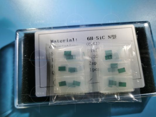
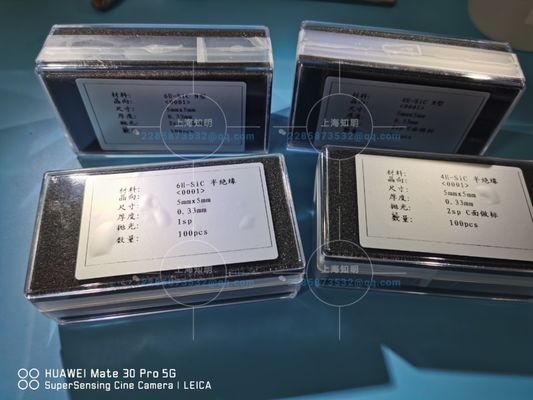
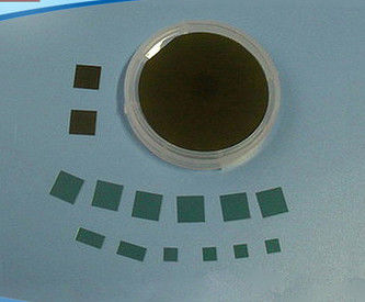
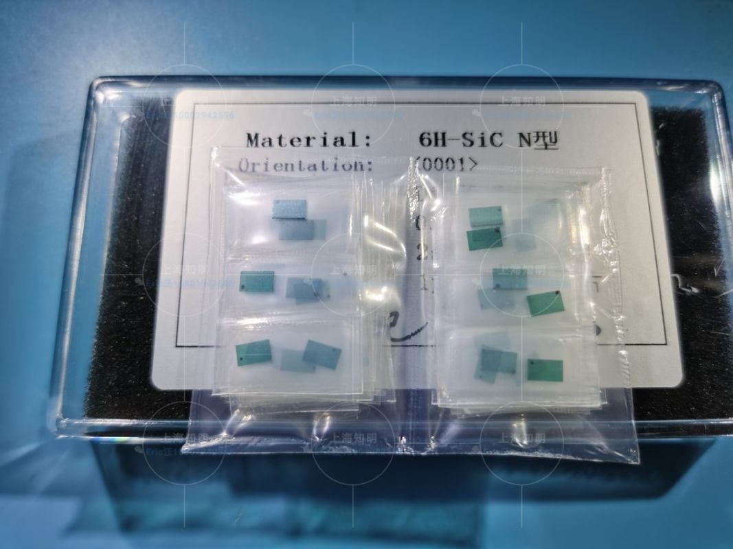
Single Crystal 5*5mm 6H-N Polished Silicon Carbide Wafer
Product Details:
| Place of Origin: | CHINA |
| Brand Name: | ZMKJ |
| Model Number: | CUSTOMIZED SIZE |
Payment & Shipping Terms:
| Minimum Order Quantity: | 1pcs |
|---|---|
| Price: | by case |
| Packaging Details: | single wafer package in 100-grade cleaning room |
| Delivery Time: | 1-6weeks |
| Payment Terms: | T/T, Western Union, MoneyGram |
| Supply Ability: | 1-50pcs/month |
|
Detail Information |
|||
| Material: | SiC Single Crystal 6H-N Type | Grade: | Test Grade |
|---|---|---|---|
| Thicnkss: | 0.35mm 0.5mm | Suraface: | Polished |
| Application: | Bearing Test | Diameter: | 2inch Or 10x10mmt, 5x10mmt: |
| Color: | Green | ||
| High Light: | Polished Silicon Carbide Wafer,6H-N Silicon Carbide Wafer,Carbide Sic Substrate Chips Wafer |
||
Product Description
Customzied size/10x10x0.5mmt/2inch/3inch/4inch/6inch 6H-N/4H-SEMI/ 4H-N SIC ingots/High purity 4H-N 4inch 6inch dia 150mm silicon carbide single crystal (sic) substrates wafersS/ Customzied as-cut sic wafers
6H-N/6H-Semi 4H HPSI 5*10mmt 10x10mmt 5*5mm polished Silicon Carbide sic substrate chips Wafer
About Silicon Carbide (SiC)Crystal
Silicon carbide (SiC), also known as carborundum, is a semiconductor containing silicon and carbon with chemical formula SiC. SiC is used in semiconductor electronics devices that operate at high temperatures or high voltages, or both.SiC is also one of the important LED components, it is a popular substrate for growing GaN devices, and it also serves as a heat spreader in high-power LEDs.
| Property | 4H-SiC, Single Crystal | 6H-SiC, Single Crystal |
| Lattice Parameters | a=3.076 Å c=10.053 Å | a=3.073 Å c=15.117 Å |
| Stacking Sequence | ABCB | ABCACB |
| Mohs Hardness | ≈9.2 | ≈9.2 |
| Density | 3.21 g/cm3 | 3.21 g/cm3 |
| Therm. Expansion Coefficient | 4-5×10⁻⁶/K | 4-5×10⁻⁶/K |
| Refraction Index @750nm |
no = 2.61 |
no = 2.60 |
| Dielectric Constant | c~9.66 | c~9.66 |
| Thermal Conductivity (N-type, 0.02 ohm.cm) |
a~4.2 W/cm·K@298K |
|
| Thermal Conductivity (Semi-insulating) |
a~4.9 W/cm·K@298K |
a~4.6 W/cm·K@298K |
| Band-gap | 3.23 eV | 3.02 eV |
| Break-Down Electrical Field | 3-5×10⁶V/cm | 3-5×10⁶V/cm |
| Saturation Drift Velocity | 2.0×10⁵m/s | 2.0×10⁵m/s |
High purity 4inch diameter Silicon Carbide (SiC) Substrate Specification
| 2inch diameter Silicon Carbide (SiC) Substrate Specification | ||||||||||
| Grade | Zero MPD Grade | Production Grade | Research Grade | Dummy Grade | ||||||
| Diameter | 50.8 mm±0.2mm | |||||||||
| Thickness | 330 μm±25μm or 430±25um | |||||||||
| Wafer Orientation | Off axis : 4.0° toward <1120> ±0.5° for 4H-N/4H-SI On axis : <0001>±0.5° for 6H-N/6H-SI/4H-N/4H-SI | |||||||||
| Micropipe Density | ≤0 cm-2 | ≤5 cm-2 | ≤15 cm-2 | ≤100 cm-2 | ||||||
| Resistivity | 4H-N | 0.015~0.028 Ω•cm | ||||||||
| 6H-N | 0.02~0.1 Ω•cm | |||||||||
| 4/6H-SI | ≥1E5 Ω·cm | |||||||||
| Primary Flat | {10-10}±5.0° | |||||||||
| Primary Flat Length | 18.5 mm±2.0 mm | |||||||||
| Secondary Flat Length | 10.0mm±2.0 mm | |||||||||
| Secondary Flat Orientation | Silicon face up: 90° CW. from Prime flat ±5.0° | |||||||||
| Edge exclusion | 1 mm | |||||||||
| TTV/Bow /Warp | ≤10μm /≤10μm /≤15μm | |||||||||
| Roughness | Polish Ra≤1 nm | |||||||||
| CMP Ra≤0.5 nm | ||||||||||
| Cracks by high intensity light | None | 1 allowed, ≤2 mm | Cumulative length ≤ 10mm, single length≤2mm | |||||||
| Hex Plates by high intensity light | Cumulative area ≤1% | Cumulative area ≤1% | Cumulative area ≤3% | |||||||
| Polytype Areas by high intensity light | None | Cumulative area ≤2% | Cumulative area ≤5% | |||||||
| Scratches by high intensity light | 3 scratches to 1×wafer diameter cumulative length | 5 scratches to 1×wafer diameter cumulative length | 5 scratches to 1×wafer diameter cumulative length | |||||||
| edge chip | None | 3 allowed, ≤0.5 mm each | 5 allowed, ≤1 mm each | |||||||
![]()
|
4H-N Type / High Purity SiC wafer/ingots
2 inch 4H N-Type SiC wafer/ingots
3 inch 4H N-Type SiC wafer 4 inch 4H N-Type SiC wafer/ingots 6 inch 4H N-Type SiC wafer/ingots |
4H Semi-insulating / High Purity SiC wafer 2 inch 4H Semi-insulating SiC wafer
3 inch 4H Semi-insulating SiC wafer 4 inch 4H Semi-insulating SiC wafer 6 inch 4H Semi-insulating SiC wafer |
|
6H N-Type SiC wafer
2 inch 6H N-Type SiC wafer/ingot |
Customzied size for 2-6inch
|
SiC Applications
Application areas
- 1 high frequency and high power electronic devices Schottky diodes, JFET, BJT, PiN,
- diodes, IGBT, MOSFET
- 2 optoelectronic devices: mainly used in GaN/SiC blue LED substrate material (GaN/SiC) LED
>Packaging – Logistcs
we concerns each details of the package , cleaning, anti-static , shock treatment .
According to the quantity and shape of the product , we will take a different packaging process! Almost by single wafer cassettes or 25pcs cassette in 100 grade cleaning room.
![]()